




惯性聚合 高效追踪和阅读你感兴趣的博客、新闻、科技资讯
阅读原文 在惯性聚合中打开

推荐订阅源

V
V2EX
奇客Solidot–传递最新科技情报
奇客Solidot–传递最新科技情报
WordPress大学
WordPress大学
罗磊的独立博客
小众软件
小众软件
I
InfoQ
Y
Y Combinator Blog
宝玉的分享
宝玉的分享
钛媒体:引领未来商业与生活新知
钛媒体:引领未来商业与生活新知
Hugging Face - Blog
Hugging Face - Blog
MyScale Blog
MyScale Blog
博客园 - 聂微东
Microsoft Security Blog
H
Help Net Security
酷 壳 – CoolShell
酷 壳 – CoolShell
博客园_首页
S
SegmentFault 最新的问题
博客园 - 三生石上(FineUI控件)
P
Proofpoint News Feed
博客园 - 司徒正美
Cyber Security Advisories - MS-ISAC
Microsoft Azure Blog
Jina AI
Jina AI
N
Netflix TechBlog - Medium

TrendForce

[News] ASE Reportedly Raises Advanced Packaging Quotes by More Than 20% in Latest AI-Driven Price Hike [News] Musk’s TeraFab Lands First Major Hire as 18-Year Intel Veteran With 18A Experience Joins as Director [Insights] Memory Spot Price Update: DRAM Spot Prices See Gains in Low-Density DDR4 and DDR3 Amid Sideways Market [News] Passive Component Prices Rise as YAGEO Reportedly Begins Broadest Capacitor Hike in Years on July 1 [News] Intel Reportedly Breaks Ground on Santa Clara Expansion for Next-Gen EUV Mask Capacity [News] World’s First Mass-Production Line for 6-/8-Inch Homoepitaxial Gallium Oxide Wafers Comes Online [News] Samsung Electro-Mechanics Lands KRW 450B 1-Year MLCC Contract as AI Spurs Long-Term Agreements [News] Raw Material Inflation Deepens: FULLTECH Hikes Glass Fiber Cloth Prices Up to 30%; VPEC Adjusts Epi Wafer Prices [News] Samsung Reportedly Restarts 1.4nm Push, Targets 2029 Mass Production to Close Gap with TSMC, Intel [News] ByteDance Reportedly Eyes Next-Gen In-House CPU for 2H27 Mass Production; May Partner With Qualcomm [News] Samsung, SK hynix 800 Trillion Won Expansion Strains Chipmaking Tool Supply, Potentially Pressures TSMC, Intel [News] Goertek-Backed 12-Inch AR Optical Wafer Fab Commenced Production [News] China Signs First Domestic Ultra Wide Bandgap Semiconductor Full-Chain Project [News] Samsung, SK hynix, Micron Face U.S. Class-Action Lawsuit Over Alleged DRAM Supply Manipulation [News] Korea’s High-Purity CO₂ Inventory Reportedly Falls Below One Month; Samsung, SK hynix Under Pressure [News] TSMC’s 2Q Margins Reportedly Near 70% amid Strong 3/5nm Demand, 3Q Revenue Seen Growing Over 10% [Sponsored Content] Where Do You Stand as AI Reshapes Industries? [News] Mapping the Micro LED Optical Interconnect Ecosystem [News] Asian Memory Makers Turn to U.S. Capital Markets: SK hynix and Kioxia Advance ADR Plans [News] Lenovo Reportedly Sees Higher Memory Prices Becoming the New Normal Into 2030 [News] TSMC on Terafab: No Shortcuts in Foundry; Confirms Next-Gen LPU Project amid Samsung Rivalry [News] TSMC N3 Tightens on AI Demand; Arizona 2nd Fab 3nm Volume Production in 2H27, Kumamoto in 2028 [News] TSMC Sees 2Q Sales Up 10% QoQ to $40.2B; Margins Rise to 65.5%–67.5%, Capex at Top End of $52–56B [News] TSMC 1Q26 Net Income Soars 58% YoY to NT$572.5B Record, EPS NT$22.08; Gross Margin Beats Forecast at 66.2% [News] Tesla AI5 Reportedly Uses SK hynix Memory, Samsung LPDDR5X; Samsung SF2T Process Applied Ahead of AI6 [News] TSMC 1Q Profit Seen Up ~50% to Record; Meta–Broadcom AI Chips Reportedly Target 2nm, CoWoS-L in 1H27 [News] San’an Announced Three Advances in Optical Communications Business [News] Intel Reportedly to Brief Staff on TeraFab Involvement in Coming Weeks, While Key Foundry Details Remain Limited [News] ASML Raises 2026 Sales Outlook to €36B–€40B on Memory, Logic Demand; South Korea Share Hits 45% [News] Chinese Startup Dishan Reportedly Develops 2nm AI Chip in Prototype Verification; Foundry Access Uncertain
[News] NVIDIA’s $20B Groq Deal Spotlights SRAM Shift—Medi...
2025-12-30 · via TrendForce


With markets staying muted over the Christmas holiday, NVIDIA made an unexpected move, agreeing to spend about $20 billion in cash to license Groq’s LPU (Language Processing Unit) technology. As highlighted by the Commercial Times, the deal signals that the AI chip leader is accelerating its push beyond traditional GPU architectures, with implications extending to how SRAM (Static Random Access Memory) is being rethought for edge AI.

While speculation continues over how NVIDIA will ultimately deploy the technology, Commercial Times reports—citing SRAM EDA tool provider iSTART—that Computing-in-Memory (CIM) chips are increasingly replacing portions of DRAM with SRAM, a design approach already adopted by Groq’s LPU. Notably, the report also flags MediaTek as another player to watch in the SRAM game, noting that its flagship Dimensity 9500 smartphone chip adopts a processing-in-memory NPU architecture.

Why SRAM Matters

As Commercial Times explains, SRAM is typically integrated within logic processes (on-chip) and supplied by foundries such as TSMC and Samsung. While it delivers superior performance and ultra-low latency, SRAM comes with trade-offs: lower integration density, higher power consumption than DRAM, and substantial die area requirements. For this reason, SRAM is often used as cache memory between processors (CPUs) and main memory, providing rapid response times for applications like L1 and L2 CPU caches.

SRAM’s advantages also extend to AI applications. According to the Economic Daily News, Groq has designed its chips without relying on external HBM, shielding them from memory supply shortages. By integrating SRAM directly on-chip, the architecture helps accelerate interactions between chatbots and other AI models, the report adds.

SRAM’s Expanding Role in AI Inference Chips

A growing number of AI inference chips and CIM architecture processors are now substituting SRAM for portions of DRAM to unlock faster access speeds and dramatically lower refresh latency, according to Commercial Times. Groq’s LPU stands as a prime example, reportedly packing a massive 230MB of SRAM onto a single chip with on-chip memory bandwidth reaching up to 80TB/s—effectively sidestepping the bandwidth bottlenecks that plague traditional DRAM and external memory.

MediaTek has taken a similar approach with the Dimensity 9500’s ultra-efficient NPU, which debuts a processing-in-memory architecture enabling AI models to run persistently. Industry analysts cited by the report note that while SRAM carries a higher total cost of ownership, it slashes data transfer latency in AI inference workloads. For edge AI devices in particular, this translates into fewer DRAM modules required and more compact system designs, the report suggests.

According to Commercial Times, these developments signal a broader shift: ASIC architectures embedding massive amounts of SRAM are gradually emerging, prompting a fundamental reassessment of the once-unchallenged HBM pathway.

Read more

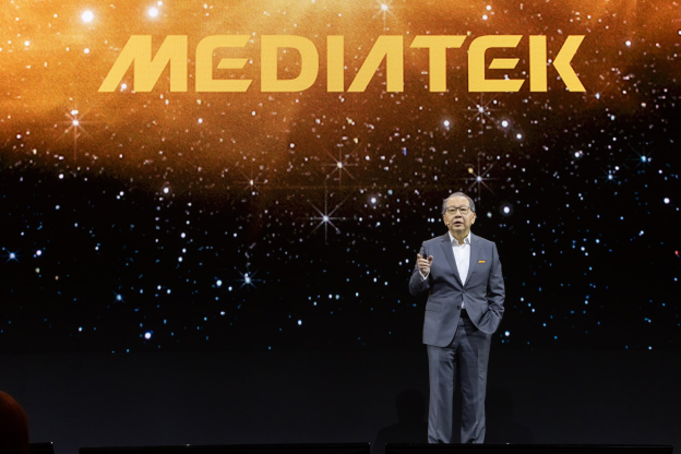
(Photo credit: MediaTek)

Please note that this article cites information from Commercial Times and the Economic Daily News.
