


惯性聚合 高效追踪和阅读你感兴趣的博客、新闻、科技资讯
阅读原文 在惯性聚合中打开

推荐订阅源

T
Threatpost
Jina AI
Jina AI
S
SegmentFault 最新的问题
博客园 - 【当耐特】
阮一峰的网络日志
阮一峰的网络日志
IT之家
IT之家
让小产品的独立变现更简单 - ezindie.com
aimingoo的专栏
aimingoo的专栏
博客园 - 叶小钗
The Cloudflare Blog
MyScale Blog
MyScale Blog
F
Full Disclosure
T
Tailwind CSS Blog
Recent Announcements
云风的 BLOG
云风的 BLOG
B
Blog
Apple Machine Learning Research
Engineering at Meta
Engineering at Meta
P
Privacy & Cybersecurity Law Blog
H
Help Net Security
A
Arctic Wolf
T
Tor Project blog
WordPress大学
WordPress大学
Cisco Talos Blog
Cisco Talos Blog
D
Darknet – Hacking Tools, Hacker News & Cyber Security
Project Zero
Project Zero
V2EX - 技术
V2EX - 技术
C
CERT Recently Published Vulnerability Notes
L
Lohrmann on Cybersecurity
CTFtime.org: upcoming CTF events
cs.AI updates on arXiv.org
Hacker News: Ask HN
Hacker News: Ask HN
有赞技术团队
有赞技术团队
Y
Y Combinator Blog
S
Securelist
OSCHINA 社区最新新闻
OSCHINA 社区最新新闻
博客园 - 三生石上(FineUI控件)
PCI Perspectives
PCI Perspectives
雷峰网
雷峰网
J
Java Code Geeks
G
GRAHAM CLULEY
D
DataBreaches.Net
C
CXSECURITY Database RSS Feed - CXSecurity.com
Attack and Defense Labs
美团技术团队
Security Archives - TechRepublic
奇客Solidot–传递最新科技情报
奇客Solidot–传递最新科技情报
D
Docker
Cloudbric
Cloudbric
L
LangChain Blog

TrendForce

[News] ASE Reportedly Raises Advanced Packaging Quotes by More Than 20% in Latest AI-Driven Price Hike [News] Musk’s TeraFab Lands First Major Hire as 18-Year Intel Veteran With 18A Experience Joins as Director [Insights] Memory Spot Price Update: DRAM Spot Prices See Gains in Low-Density DDR4 and DDR3 Amid Sideways Market [News] Passive Component Prices Rise as YAGEO Reportedly Begins Broadest Capacitor Hike in Years on July 1 [News] Intel Reportedly Breaks Ground on Santa Clara Expansion for Next-Gen EUV Mask Capacity [News] Samsung Electro-Mechanics Lands KRW 450B 1-Year MLCC Contract as AI Spurs Long-Term Agreements [News] Raw Material Inflation Deepens: FULLTECH Hikes Glass Fiber Cloth Prices Up to 30%; VPEC Adjusts Epi Wafer Prices [News] Samsung Reportedly Restarts 1.4nm Push, Targets 2029 Mass Production to Close Gap with TSMC, Intel [News] ByteDance Reportedly Eyes Next-Gen In-House CPU for 2H27 Mass Production; May Partner With Qualcomm [News] Samsung, SK hynix 800 Trillion Won Expansion Strains Chipmaking Tool Supply, Potentially Pressures TSMC, Intel [News] Goertek-Backed 12-Inch AR Optical Wafer Fab Commenced Production [News] China Signs First Domestic Ultra Wide Bandgap Semiconductor Full-Chain Project [News] Samsung, SK hynix, Micron Face U.S. Class-Action Lawsuit Over Alleged DRAM Supply Manipulation [News] Korea’s High-Purity CO₂ Inventory Reportedly Falls Below One Month; Samsung, SK hynix Under Pressure [News] TSMC’s 2Q Margins Reportedly Near 70% amid Strong 3/5nm Demand, 3Q Revenue Seen Growing Over 10% [Sponsored Content] Where Do You Stand as AI Reshapes Industries? [News] Mapping the Micro LED Optical Interconnect Ecosystem [News] Asian Memory Makers Turn to U.S. Capital Markets: SK hynix and Kioxia Advance ADR Plans [News] Lenovo Reportedly Sees Higher Memory Prices Becoming the New Normal Into 2030 [News] TSMC on Terafab: No Shortcuts in Foundry; Confirms Next-Gen LPU Project amid Samsung Rivalry [News] TSMC N3 Tightens on AI Demand; Arizona 2nd Fab 3nm Volume Production in 2H27, Kumamoto in 2028 [News] TSMC Sees 2Q Sales Up 10% QoQ to $40.2B; Margins Rise to 65.5%–67.5%, Capex at Top End of $52–56B [News] TSMC 1Q26 Net Income Soars 58% YoY to NT$572.5B Record, EPS NT$22.08; Gross Margin Beats Forecast at 66.2% [News] Tesla AI5 Reportedly Uses SK hynix Memory, Samsung LPDDR5X; Samsung SF2T Process Applied Ahead of AI6 [News] TSMC 1Q Profit Seen Up ~50% to Record; Meta–Broadcom AI Chips Reportedly Target 2nm, CoWoS-L in 1H27 [News] San’an Announced Three Advances in Optical Communications Business [News] Intel Reportedly to Brief Staff on TeraFab Involvement in Coming Weeks, While Key Foundry Details Remain Limited [News] ASML Raises 2026 Sales Outlook to €36B–€40B on Memory, Logic Demand; South Korea Share Hits 45% [News] Chinese Startup Dishan Reportedly Develops 2nm AI Chip in Prototype Verification; Foundry Access Uncertain [News] Musk Confirms AI5 Tape-Out, but Wrong TSMC Tag Triggers Social Media Mix-Up [News] China Reportedly Sees Record 2025 Chip Tool Imports from Singapore, Malaysia; U.S. Hit Lowest Since 2017 [Insights] Memory Spot Price Update: DRAM Spot Sellers Hold Firm Ahead of Mid-April Pricing, DDR4 Edges Lower 0.48% [News] HBM4 Strategies Diverge: Samsung Reportedly Chases 80% 1c DRAM Yield While SK hynix Trims Shipments by 30% [News] Korea Challenges Intel on Glass Substrate Standards as Absolics, Samsung Accelerate Commercialization [Insights] NVIDIA’s US$2B Marvell Deal: What’s the Strategic Significance for CPO and AI Interconnects? [News] Samsung Reportedly Lifts HBM4 Logic Die Prices by 40–50% Amid AI Boom; 4nm at Full Capacity [News] Huawei Takes Early Lead in Horizontal Foldable Race vs Samsung and Apple, Eyes April Pura X Max Launch [News] China Reportedly Closes AI Performance Gap with U.S., Stanford Report Says; Anthropic Leads by Just 2.7% [News] Samsung 2nm Yields Reportedly at ~55%, Below Mass Production Threshold; Qualcomm May Opt for TSMC [Insights] Memory Spot Price Update: DDR4 Spot Prices Climb as Samsung Holds EOL Line [News] TSMC May Fast-Track 1.4nm at Central Taiwan Science Park as 2nm Yields Reportedly Beat Expectations [News] Micron Reportedly Weighs Acquiring PSMC 12-Inch Tongluo Fab, With Multiple Partners Also Interested [News] ASUS to Raise Prices on Selected PC Lines from Jan. 5 Amid Memory Cost Surge, Following Dell [News] 2025 Tech Layoffs: Meta, Amazon, Microsoft and Others Cut Tens of Thousands of Roles [News] Sony, Microsoft Reportedly Weigh Delaying Next-Gen Game Consoles Beyond 2028 Amid Memory Price Surge [News] Samsung Reportedly Plans 50% HBM Capacity Surge in 2026, Spotlight on HBM4 [News] China Diversification Reportedly Lifts Mature-Node Foundries UMC, VIS, PSMC Despite Tariff Delay [News] Samsung, SK hynix Escape Worst-Case as China VEU Ends: Annual Review Risks Loom [News] TSMC Advanced-Node Materials Reportedly Found at Lo’s Residence Amid Controversial Intel Hire [News] NVIDIA’s $20B Groq Deal Spotlights SRAM Shift—MediaTek NPU Already On Board [News] Chinese Scientists Achieved New Breakthrough in Next-Gen Optical Computing Chips [News] Five-Year-Old Chinese EDA Firm Univista Sets Sights on IPO, Led by Ex-Synopsys and Cadence Team [News] Samsung Reportedly Pushes In-House CPU and GPU for Exynos 2800 to Cut Qualcomm, AMD Reliance [News] SK hynix Reportedly Plans First U.S. 2.5D Packaging Line, Eyes Turnkey HBM to Challenge TSMC [News] TSMC Reportedly to Raise Sub-3nm Prices 3-10% in 2026, Plans Hikes Through 2029 [News] Samsung Emerges as Potential Second Foundry for NVIDIA Alongside TSMC After Groq Licensing Deal [News] 7.0 Quake Hits: TSMC Nears Full Production, Sector Losses Reportedly Tens of Billions NTD [News] SLC-Based AI SSDs Gain Traction as SK hynix and Kioxia Accelerate Development With NVIDIA [News] NVIDIA Reportedly Denies USD 20B Groq Acquisition Rumors
[News] World’s First Mass-Production Line for 6-/8-Inch Homoepitaxial Gallium Oxide Wafers Comes Online
TrendForce · 2026-07-01 · via TrendForce


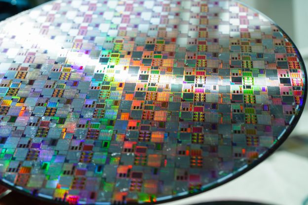
On June 24, 2026, Hangzhou Garen Semiconductor announced a major commercialization milestone: the company has successfully established the world’s first mass-production line compatible with both 6-inch and 8-inch homoepitaxial gallium oxide wafers. The company has already delivered 6-inch (100)-oriented homoepitaxial gallium oxide wafers to leading chipmakers, marking its entry into stable volume production and supply.

The global gallium oxide industry has long been constrained by small wafer sizes, limited production capacity, and poor uniformity. Most commercially available products have been restricted to 2-inch to 4-inch wafers, making large-scale manufacturing of advanced power devices difficult.

By establishing a complete mass-production process, Garen claims to have overcome key commercialization barriers and become the world’s first—and currently only—supplier capable of commercially delivering 6-inch homoepitaxial gallium oxide wafers.

The production line combines Garen’s proprietary cast-growth single-crystal technology with an optimized MOCVD epitaxy process. The in-house crystal growth method enables the production of ultra-thick gallium oxide crystals, while an ultra-thin substrate process increases substrate output by three to four times compared with conventional approaches.

The technology also significantly reduces iridium consumption, lowering substrate costs by more than 80% per wafer and helping cut material costs for downstream device manufacturers.

Product qualification data released by the company show that its 6-inch homoepitaxial gallium oxide wafers feature epitaxial layers exceeding 10μm in thickness, with thickness variation below 1%. The high level of uniformity is expected to support improved yields for high-performance devices designed for high-voltage, high-frequency, and high-temperature applications.

On the manufacturing side, Garen has established a fully integrated production chain covering single-crystal growth, substrate processing, and homoepitaxy. The 6-/8-inch compatible production line has reportedly achieved stable and controllable batch quality. In addition to long-term supply agreements with major domestic chipmakers, the company said that several overseas enterprises and research institutions have also placed orders, accelerating commercial adoption.

Gallium oxide, an ultra-wide-bandgap semiconductor material, offers high breakdown field strength, low conduction losses, and strong high-temperature performance. It is considered a promising material for applications including high-voltage power grids, electric vehicles, photovoltaic energy storage systems, and advanced RF communications.

The transition to larger wafer sizes is expected to significantly improve manufacturing efficiency, with an 8-inch wafer capable of producing roughly four times as many chips as a 4-inch wafer, enhancing the economics of large-scale production.

(Photo credit: FREEPIK)