

惯性聚合 高效追踪和阅读你感兴趣的博客、新闻、科技资讯
阅读原文 在惯性聚合中打开

推荐订阅源

酷 壳 – CoolShell
酷 壳 – CoolShell
G
Google Developers Blog
L
LangChain Blog
Y
Y Combinator Blog
Vercel News
Vercel News
WordPress大学
WordPress大学
大猫的无限游戏
大猫的无限游戏
博客园 - Franky
V
Visual Studio Blog
小众软件
小众软件
月光博客
月光博客
A
About on SuperTechFans
H
Hackread – Cybersecurity News, Data Breaches, AI and More
T
The Blog of Author Tim Ferriss
有赞技术团队
有赞技术团队
M
MIT News - Artificial intelligence
阮一峰的网络日志
阮一峰的网络日志
Last Week in AI
Last Week in AI
博客园 - 【当耐特】
让小产品的独立变现更简单 - ezindie.com
MongoDB | Blog
MongoDB | Blog
Jina AI
Jina AI
美团技术团队
量子位

TrendForce

[News] ASE Reportedly Raises Advanced Packaging Quotes by More Than 20% in Latest AI-Driven Price Hike [News] Musk’s TeraFab Lands First Major Hire as 18-Year Intel Veteran With 18A Experience Joins as Director [Insights] Memory Spot Price Update: DRAM Spot Prices See Gains in Low-Density DDR4 and DDR3 Amid Sideways Market [News] Passive Component Prices Rise as YAGEO Reportedly Begins Broadest Capacitor Hike in Years on July 1 [News] Intel Reportedly Breaks Ground on Santa Clara Expansion for Next-Gen EUV Mask Capacity [News] Samsung Electro-Mechanics Lands KRW 450B 1-Year MLCC Contract as AI Spurs Long-Term Agreements [News] Raw Material Inflation Deepens: FULLTECH Hikes Glass Fiber Cloth Prices Up to 30%; VPEC Adjusts Epi Wafer Prices [News] Samsung Reportedly Restarts 1.4nm Push, Targets 2029 Mass Production to Close Gap with TSMC, Intel [News] ByteDance Reportedly Eyes Next-Gen In-House CPU for 2H27 Mass Production; May Partner With Qualcomm [News] Samsung, SK hynix 800 Trillion Won Expansion Strains Chipmaking Tool Supply, Potentially Pressures TSMC, Intel [News] Goertek-Backed 12-Inch AR Optical Wafer Fab Commenced Production [News] China Signs First Domestic Ultra Wide Bandgap Semiconductor Full-Chain Project [News] Samsung, SK hynix, Micron Face U.S. Class-Action Lawsuit Over Alleged DRAM Supply Manipulation [News] Korea’s High-Purity CO₂ Inventory Reportedly Falls Below One Month; Samsung, SK hynix Under Pressure [News] TSMC’s 2Q Margins Reportedly Near 70% amid Strong 3/5nm Demand, 3Q Revenue Seen Growing Over 10% [Sponsored Content] Where Do You Stand as AI Reshapes Industries? [News] Mapping the Micro LED Optical Interconnect Ecosystem [News] Asian Memory Makers Turn to U.S. Capital Markets: SK hynix and Kioxia Advance ADR Plans [News] Lenovo Reportedly Sees Higher Memory Prices Becoming the New Normal Into 2030 [News] TSMC on Terafab: No Shortcuts in Foundry; Confirms Next-Gen LPU Project amid Samsung Rivalry [News] TSMC N3 Tightens on AI Demand; Arizona 2nd Fab 3nm Volume Production in 2H27, Kumamoto in 2028 [News] TSMC Sees 2Q Sales Up 10% QoQ to $40.2B; Margins Rise to 65.5%–67.5%, Capex at Top End of $52–56B [News] TSMC 1Q26 Net Income Soars 58% YoY to NT$572.5B Record, EPS NT$22.08; Gross Margin Beats Forecast at 66.2% [News] Tesla AI5 Reportedly Uses SK hynix Memory, Samsung LPDDR5X; Samsung SF2T Process Applied Ahead of AI6 [News] TSMC 1Q Profit Seen Up ~50% to Record; Meta–Broadcom AI Chips Reportedly Target 2nm, CoWoS-L in 1H27 [News] San’an Announced Three Advances in Optical Communications Business [News] Intel Reportedly to Brief Staff on TeraFab Involvement in Coming Weeks, While Key Foundry Details Remain Limited [News] ASML Raises 2026 Sales Outlook to €36B–€40B on Memory, Logic Demand; South Korea Share Hits 45% [News] Chinese Startup Dishan Reportedly Develops 2nm AI Chip in Prototype Verification; Foundry Access Uncertain [News] Musk Confirms AI5 Tape-Out, but Wrong TSMC Tag Triggers Social Media Mix-Up
[News] World’s First Mass-Production Line for 6-/8-Inch H...
TrendForce · 2026-07-01 · via TrendForce


On June 24, 2026, Hangzhou Garen Semiconductor announced a major commercialization milestone: the company has successfully established the world’s first mass-production line compatible with both 6-inch and 8-inch homoepitaxial gallium oxide wafers. The company has already delivered 6-inch (100)-oriented homoepitaxial gallium oxide wafers to leading chipmakers, marking its entry into stable volume production and supply.

The global gallium oxide industry has long been constrained by small wafer sizes, limited production capacity, and poor uniformity. Most commercially available products have been restricted to 2-inch to 4-inch wafers, making large-scale manufacturing of advanced power devices difficult.

By establishing a complete mass-production process, Garen claims to have overcome key commercialization barriers and become the world’s first—and currently only—supplier capable of commercially delivering 6-inch homoepitaxial gallium oxide wafers.

The production line combines Garen’s proprietary cast-growth single-crystal technology with an optimized MOCVD epitaxy process. The in-house crystal growth method enables the production of ultra-thick gallium oxide crystals, while an ultra-thin substrate process increases substrate output by three to four times compared with conventional approaches.

The technology also significantly reduces iridium consumption, lowering substrate costs by more than 80% per wafer and helping cut material costs for downstream device manufacturers.

Product qualification data released by the company show that its 6-inch homoepitaxial gallium oxide wafers feature epitaxial layers exceeding 10μm in thickness, with thickness variation below 1%. The high level of uniformity is expected to support improved yields for high-performance devices designed for high-voltage, high-frequency, and high-temperature applications.

On the manufacturing side, Garen has established a fully integrated production chain covering single-crystal growth, substrate processing, and homoepitaxy. The 6-/8-inch compatible production line has reportedly achieved stable and controllable batch quality. In addition to long-term supply agreements with major domestic chipmakers, the company said that several overseas enterprises and research institutions have also placed orders, accelerating commercial adoption.

Gallium oxide, an ultra-wide-bandgap semiconductor material, offers high breakdown field strength, low conduction losses, and strong high-temperature performance. It is considered a promising material for applications including high-voltage power grids, electric vehicles, photovoltaic energy storage systems, and advanced RF communications.

The transition to larger wafer sizes is expected to significantly improve manufacturing efficiency, with an 8-inch wafer capable of producing roughly four times as many chips as a 4-inch wafer, enhancing the economics of large-scale production.

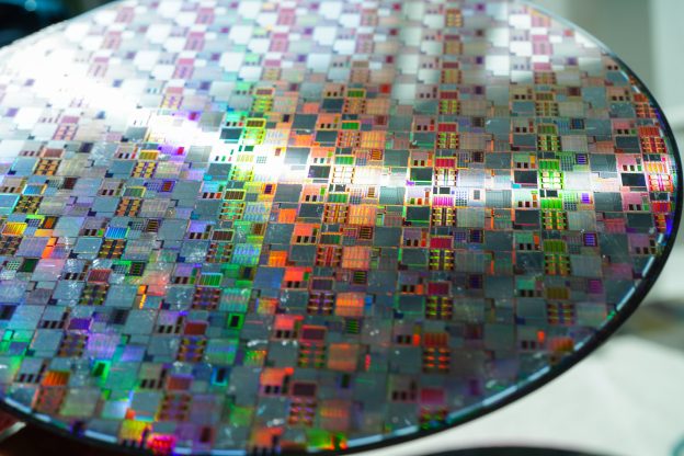
(Photo credit: FREEPIK)