


惯性聚合 高效追踪和阅读你感兴趣的博客、新闻、科技资讯
阅读原文 在惯性聚合中打开

推荐订阅源

B
Blog
A
About on SuperTechFans
Microsoft Security Blog
Y
Y Combinator Blog
罗磊的独立博客
J
Java Code Geeks
人人都是产品经理
人人都是产品经理
MongoDB | Blog
MongoDB | Blog
The GitHub Blog
The GitHub Blog
G
Google Developers Blog
U
Unit 42
Microsoft Azure Blog
博客园 - Franky
Jina AI
Jina AI
F
Fortinet All Blogs
H
Help Net Security
B
Blog RSS Feed
H
Hackread – Cybersecurity News, Data Breaches, AI and More
Last Week in AI
Last Week in AI
博客园 - 司徒正美
云风的 BLOG
云风的 BLOG
M
MIT News - Artificial intelligence
C
Check Point Blog
GbyAI
GbyAI

TrendForce

[News] ASE Reportedly Raises Advanced Packaging Quotes by More Than 20% in Latest AI-Driven Price Hike [News] Musk’s TeraFab Lands First Major Hire as 18-Year Intel Veteran With 18A Experience Joins as Director [Insights] Memory Spot Price Update: DRAM Spot Prices See Gains in Low-Density DDR4 and DDR3 Amid Sideways Market [News] Passive Component Prices Rise as YAGEO Reportedly Begins Broadest Capacitor Hike in Years on July 1 [News] World’s First Mass-Production Line for 6-/8-Inch Homoepitaxial Gallium Oxide Wafers Comes Online [News] Samsung Electro-Mechanics Lands KRW 450B 1-Year MLCC Contract as AI Spurs Long-Term Agreements [News] Raw Material Inflation Deepens: FULLTECH Hikes Glass Fiber Cloth Prices Up to 30%; VPEC Adjusts Epi Wafer Prices [News] Samsung Reportedly Restarts 1.4nm Push, Targets 2029 Mass Production to Close Gap with TSMC, Intel [News] ByteDance Reportedly Eyes Next-Gen In-House CPU for 2H27 Mass Production; May Partner With Qualcomm [News] Samsung, SK hynix 800 Trillion Won Expansion Strains Chipmaking Tool Supply, Potentially Pressures TSMC, Intel [News] Goertek-Backed 12-Inch AR Optical Wafer Fab Commenced Production [News] China Signs First Domestic Ultra Wide Bandgap Semiconductor Full-Chain Project [News] Samsung, SK hynix, Micron Face U.S. Class-Action Lawsuit Over Alleged DRAM Supply Manipulation [News] Korea’s High-Purity CO₂ Inventory Reportedly Falls Below One Month; Samsung, SK hynix Under Pressure [News] TSMC’s 2Q Margins Reportedly Near 70% amid Strong 3/5nm Demand, 3Q Revenue Seen Growing Over 10% [Sponsored Content] Where Do You Stand as AI Reshapes Industries? [News] Mapping the Micro LED Optical Interconnect Ecosystem [News] Asian Memory Makers Turn to U.S. Capital Markets: SK hynix and Kioxia Advance ADR Plans [News] Lenovo Reportedly Sees Higher Memory Prices Becoming the New Normal Into 2030 [News] TSMC on Terafab: No Shortcuts in Foundry; Confirms Next-Gen LPU Project amid Samsung Rivalry [News] TSMC N3 Tightens on AI Demand; Arizona 2nd Fab 3nm Volume Production in 2H27, Kumamoto in 2028 [News] TSMC Sees 2Q Sales Up 10% QoQ to $40.2B; Margins Rise to 65.5%–67.5%, Capex at Top End of $52–56B [News] TSMC 1Q26 Net Income Soars 58% YoY to NT$572.5B Record, EPS NT$22.08; Gross Margin Beats Forecast at 66.2% [News] Tesla AI5 Reportedly Uses SK hynix Memory, Samsung LPDDR5X; Samsung SF2T Process Applied Ahead of AI6 [News] TSMC 1Q Profit Seen Up ~50% to Record; Meta–Broadcom AI Chips Reportedly Target 2nm, CoWoS-L in 1H27 [News] San’an Announced Three Advances in Optical Communications Business [News] Intel Reportedly to Brief Staff on TeraFab Involvement in Coming Weeks, While Key Foundry Details Remain Limited [News] ASML Raises 2026 Sales Outlook to €36B–€40B on Memory, Logic Demand; South Korea Share Hits 45% [News] Chinese Startup Dishan Reportedly Develops 2nm AI Chip in Prototype Verification; Foundry Access Uncertain [News] Musk Confirms AI5 Tape-Out, but Wrong TSMC Tag Triggers Social Media Mix-Up
[News] Intel Reportedly Breaks Ground on Santa Clara Expa...
TrendForce · 2026-07-01 · via TrendForce


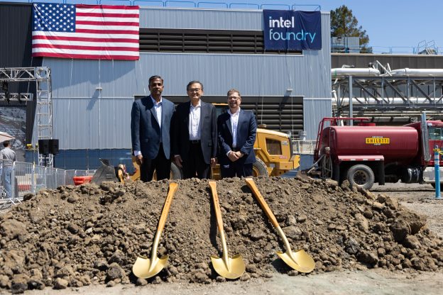
As interest in Intel’s foundry services continues to grow among a broader range of tech giants like Apple and NVIDIA, the chipmaker is accelerating its U.S. manufacturing buildout. According to Wccftech, Intel has officially broken ground on the latest expansion of its Santa Clara, California campus, with CEO Lip-Bu Tan and other senior executives attending the ceremony.

The expansion project was originally scheduled to begin in mid-2026, with the latest groundbreaking indicating that the timeline remains on track, the report adds.

Separately, policy timing could add further pressure to the buildout schedule, with a previous Tom’s Hardware report noting that semiconductor and advanced manufacturing projects must break ground by December 31, 2026, to qualify for the 35% Investment Tax Credit, and that projects initiated in 2027 or later will no longer be eligible for the incentive.

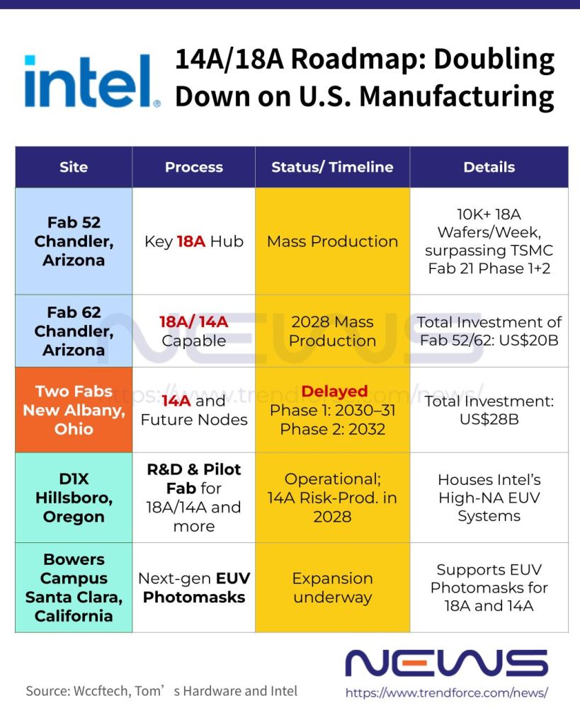
According to the San Francisco Business Times, Intel’s Santa Clara Bowers Campus development spans a 107,000-square-foot site and will include two three-story buildings dedicated to manufacturing, fabrication, and central utility operations. Wccftech adds that the site will support the production of EUV photomasks (reticles) critical to next-generation process nodes, including 18A-P and 14A.

Intel’s U.S. Expansion Roadmap in Focus

As Intel ramps up its 18A and 14A efforts, Fab 52 at the company’s Ocotillo campus in Chandler is set to serve as a key manufacturing backbone, according to Tom’s Hardware. The facility entered full-scale production in October 2025 as Intel’s first high-volume 18A site, initially producing Panther Lake compute tiles before expanding to Clearwater Forest later this year.

Notably, the report, citing CNBC, also highlights that Fab 52 is designed to support more than 10,000 Intel 18A wafer starts per week. At full ramp, this reportedly translates to roughly 40,000 wafer starts per month—exceeding the combined output of TSMC’s Fab 21 Phase 1 and Phase 2 in Arizona.

The next major Arizona expansion phase would be Fab 62, which is expected to enter production around 2028, according to Tom’s Hardware. While Intel has not disclosed its process node, Fab 62 is expected to provide flexibility to support either 14A production if Ohio falls behind schedule, or additional 18A capacity should demand outpace expectations, the report suggests.

Against this backdrop, Ohio, meanwhile, remains the most delayed project in Intel’s pipeline. After breaking ground in 2022 on a US$28 billion investment, the company has pushed Phase 1 completion to 2030 with operations in 2030–2031, followed by Phase 2 production in 2032.
Read more

(Photo credit: Intel)

Please note that this article cites information from WccftechTom’s Hardware, San Francisco Business Times and CNBC.