


惯性聚合 高效追踪和阅读你感兴趣的博客、新闻、科技资讯
阅读原文 在惯性聚合中打开

推荐订阅源

爱范儿
爱范儿
让小产品的独立变现更简单 - ezindie.com
WordPress大学
WordPress大学
Y
Y Combinator Blog
I
InfoQ
美团技术团队
罗磊的独立博客
B
Blog RSS Feed
GbyAI
GbyAI
小众软件
小众软件
IT之家
IT之家
Engineering at Meta
Engineering at Meta
Blog — PlanetScale
Blog — PlanetScale
V
V2EX
Last Week in AI
Last Week in AI
酷 壳 – CoolShell
酷 壳 – CoolShell
Jina AI
Jina AI
MyScale Blog
MyScale Blog
博客园 - 聂微东
Microsoft Security Blog
博客园 - 【当耐特】
Apple Machine Learning Research
The GitHub Blog
The GitHub Blog
T
The Blog of Author Tim Ferriss

TrendForce

[News] ASE Reportedly Raises Advanced Packaging Quotes by More Than 20% in Latest AI-Driven Price Hike [News] Musk’s TeraFab Lands First Major Hire as 18-Year Intel Veteran With 18A Experience Joins as Director [Insights] Memory Spot Price Update: DRAM Spot Prices See Gains in Low-Density DDR4 and DDR3 Amid Sideways Market [News] Passive Component Prices Rise as YAGEO Reportedly Begins Broadest Capacitor Hike in Years on July 1 [News] Intel Reportedly Breaks Ground on Santa Clara Expansion for Next-Gen EUV Mask Capacity [News] World’s First Mass-Production Line for 6-/8-Inch Homoepitaxial Gallium Oxide Wafers Comes Online [News] Samsung Electro-Mechanics Lands KRW 450B 1-Year MLCC Contract as AI Spurs Long-Term Agreements [News] Raw Material Inflation Deepens: FULLTECH Hikes Glass Fiber Cloth Prices Up to 30%; VPEC Adjusts Epi Wafer Prices [News] Samsung Reportedly Restarts 1.4nm Push, Targets 2029 Mass Production to Close Gap with TSMC, Intel [News] ByteDance Reportedly Eyes Next-Gen In-House CPU for 2H27 Mass Production; May Partner With Qualcomm [News] Samsung, SK hynix 800 Trillion Won Expansion Strains Chipmaking Tool Supply, Potentially Pressures TSMC, Intel [News] Goertek-Backed 12-Inch AR Optical Wafer Fab Commenced Production [News] Samsung, SK hynix, Micron Face U.S. Class-Action Lawsuit Over Alleged DRAM Supply Manipulation [News] Korea’s High-Purity CO₂ Inventory Reportedly Falls Below One Month; Samsung, SK hynix Under Pressure [News] TSMC’s 2Q Margins Reportedly Near 70% amid Strong 3/5nm Demand, 3Q Revenue Seen Growing Over 10% [Sponsored Content] Where Do You Stand as AI Reshapes Industries? [News] Mapping the Micro LED Optical Interconnect Ecosystem [News] Asian Memory Makers Turn to U.S. Capital Markets: SK hynix and Kioxia Advance ADR Plans [News] Lenovo Reportedly Sees Higher Memory Prices Becoming the New Normal Into 2030 [News] TSMC on Terafab: No Shortcuts in Foundry; Confirms Next-Gen LPU Project amid Samsung Rivalry [News] TSMC N3 Tightens on AI Demand; Arizona 2nd Fab 3nm Volume Production in 2H27, Kumamoto in 2028 [News] TSMC Sees 2Q Sales Up 10% QoQ to $40.2B; Margins Rise to 65.5%–67.5%, Capex at Top End of $52–56B [News] TSMC 1Q26 Net Income Soars 58% YoY to NT$572.5B Record, EPS NT$22.08; Gross Margin Beats Forecast at 66.2% [News] Tesla AI5 Reportedly Uses SK hynix Memory, Samsung LPDDR5X; Samsung SF2T Process Applied Ahead of AI6 [News] TSMC 1Q Profit Seen Up ~50% to Record; Meta–Broadcom AI Chips Reportedly Target 2nm, CoWoS-L in 1H27 [News] San’an Announced Three Advances in Optical Communications Business [News] Intel Reportedly to Brief Staff on TeraFab Involvement in Coming Weeks, While Key Foundry Details Remain Limited [News] ASML Raises 2026 Sales Outlook to €36B–€40B on Memory, Logic Demand; South Korea Share Hits 45% [News] Chinese Startup Dishan Reportedly Develops 2nm AI Chip in Prototype Verification; Foundry Access Uncertain [News] Musk Confirms AI5 Tape-Out, but Wrong TSMC Tag Triggers Social Media Mix-Up
[News] China Signs First Domestic Ultra Wide Bandgap Semi...
TrendForce · 2026-06-30 · via TrendForce


China’s Henan provincial government website revealed that Zhengzhou High-tech Zone signed an investment agreement with Sino Powder (Henan) on June 26, establishing the company’s ultra wide bandgap semiconductor material production base.

The project is described as China’s first integrated ultra wide bandgap semiconductor industrial chain, filling a key gap in Henan’s superhard materials ecosystem by extending into high-end semiconductor substrates. Home to one of the world’s largest synthetic diamond industrial clusters, Henan aims to leverage the project to accelerate the transition of its traditional diamond industry toward advanced semiconductor materials.

Ultra wide bandgap semiconductors are based on ultra wide bandgap materials such as diamond and gallium oxide, which offer exceptional physical properties including a wide bandgap, high breakdown electric field, and superior thermal conductivity. Often referred to as the “ultimate semiconductor materials,” they are expected to support applications ranging from AI chip thermal management and 5G/6G communications to electric vehicle power electronics and advanced biomedical equipment.

With a total investment of CNY 1.5 billion (approximately USD 210 million), the project will build a complete industrial chain spanning equipment manufacturing, single-crystal growth, epitaxy processing, and packaging substrates, leveraging the company’s proprietary LPPHT micro/nanodiamond production technology. The facility will be equipped with 500 MPCVD systems for mass production of 2-inch to 4-inch single-crystal diamond wafers, alongside 50 production lines for spherical diamond powder.

Under the construction roadmap, the first 200 MPCVD systems are scheduled to enter operation by the end of 2026. Once fully ramped, the project is expected to generate annual output value of approximately CNY 3 billion within three years.

Backed by Central South University, Sino Powder is among the few Chinese companies capable of providing a fully localized supply chain for diamond semiconductor materials. Earlier this March, the company established its ultra wide bandgap semiconductor materials R&D center in Zhengzhou High-tech Zone. The newly signed production base marks the next step from laboratory research to industrial-scale manufacturing.

According to the project leader, the facility will focus on the commercialization of micro- and nanodiamond semiconductor materials while addressing the key challenge of large-scale production of high-end diamond substrates.

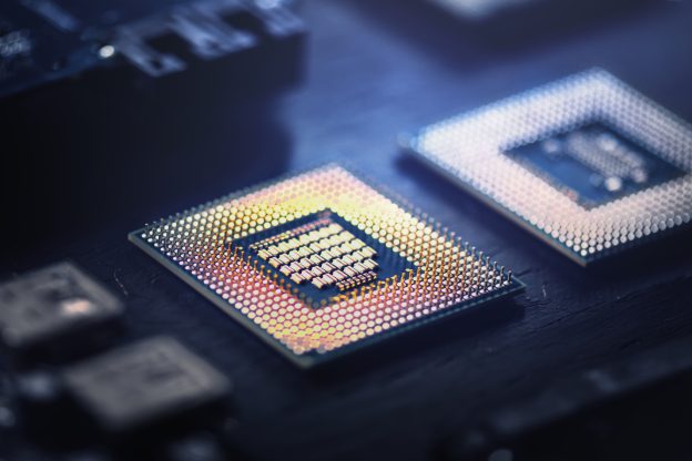
(Photo credit: FREEPIK)