





Huawei has proposed a new semiconductor development framework called the “Tau scaling law,” framing it as an alternative method to improve chip performance as Moore’s law becomes harder to sustain.
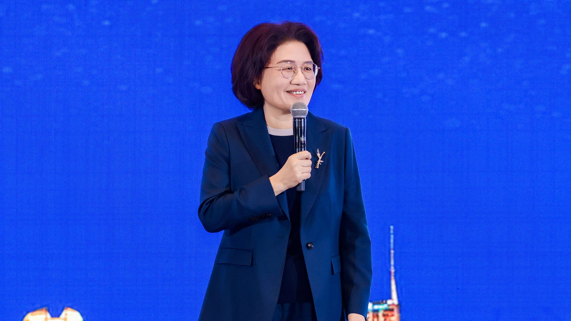
The proposal was introduced on May 25 at the IEEE International Symposium on Circuits and Systems in Shanghai by He Tingbo, chairwoman of Huawei’s scientist committee and president of its semiconductor business department. In her keynote, she described Tau scaling as a shift from geometric scaling, the traditional method of shrinking transistors, to time-based scaling, where chip performance is improved by reducing signal delay across devices, circuits, chips, and systems.
“Losing geometric scaling does not mean losing time scaling,” He said.
She added that one core technology under this approach is LogicFolding, an architecture designed to shorten critical wiring paths, reduce signal propagation delay, and improve transistor density and circuit performance. The company said Kirin chips scheduled for launch in fall and winter 2026 will be the first to adopt LogicFolding.
Dubbed “Her’s law” by He’s peers, Tau scaling is less about shrinking the chip, as Moore’s law is, and more about shortening the journey inside it. By shifting the emphasis to architecture and signal efficiency, the approach could reduce dependence on the most advanced lithography tools, though not eliminate it.
Traditional semiconductor progress has long been measured by how small transistors can be made and how many can be packed onto a chip. Huawei’s proposition focuses instead on how efficiently signals and data move. In theory, shorter signal paths can reduce latency and improve performance, even if the underlying manufacturing process does not match the most advanced global nodes.
According to He, high-end chips based on Tau scaling could reach transistor density equivalent to 14 angstroms, or 1.4-nm, processes by 2031.
This does not necessarily mean Huawei expects to manufacture true 1.4-nm chips by then. A more precise reading is that it aims to achieve density comparable to future 1.4-nm-class processes through architecture, circuit design, and system-level optimization.
With LogicFolding, Huawei intends to switch its Kirin chips from a single-layer to a double-layer structure. By stacking and rearranging parts of the chip, Huawei believes the vertical design can increase density and enhance performance, even if the underlying manufacturing process has not advanced by the same amount under geometric scaling.
“Before LogicFolding, it took three years to lift transistor density from 126 to 155 million transistors per square millimeter,” He said. “In 2026, LogicFolding takes it all the way to 238 million transistors per square millimeter, in one single step.”
The global benchmark is already moving in that direction. TSMC unveiled its A14 process, a 1.4-nm-class technology, in 2025 and said it is planned to enter production in 2028. Other leading chipmakers, including Intel and Samsung, are also pursuing next-generation nodes around the 2-nm and angstrom-class range.
Huawei’s target is therefore ambitious, though it would still need external validation through commercial chips, measurable density gains, production yields, and real-world performance.
The announcement comes as China continues to face constraints in advanced chipmaking due to US and allied export controls that have limited the country’s near-term ability to produce chips beyond the 7-nm node. Huawei and others in China’s broader semiconductor sector have been looking for ways to sustain chip advances amid these restrictions, with localization of semiconductor design and manufacturing among Beijing’s priorities.
The proposal is therefore significant because it builds on Huawei’s broader role in China’s artificial intelligence and semiconductor self-reliance push. Huawei has often been cited as a central player in China’s AI chip self-reliance drive, including through its work with domestic chipmakers, while studies note that Chinese AI chips still generally lag Nvidia in performance.
Tau scaling also sits alongside other approaches aimed at extending computing performance beyond Moore’s law, including neuromorphic computing and quantum computing.
此内容由惯性聚合(RSS阅读器)自动聚合整理,仅供阅读参考。 原文来自 — 版权归原作者所有。