



惯性聚合 高效追踪和阅读你感兴趣的博客、新闻、科技资讯
阅读原文 在惯性聚合中打开

推荐订阅源

D
DataBreaches.Net
罗磊的独立博客
雷峰网
雷峰网
量子位
V
Visual Studio Blog
Vercel News
Vercel News
freeCodeCamp Programming Tutorials: Python, JavaScript, Git & More
The Cloudflare Blog
钛媒体:引领未来商业与生活新知
钛媒体:引领未来商业与生活新知
宝玉的分享
宝玉的分享
月光博客
月光博客
Martin Fowler
Martin Fowler
aimingoo的专栏
aimingoo的专栏
H
Hackread – Cybersecurity News, Data Breaches, AI and More
Microsoft Security Blog
博客园 - 叶小钗
腾讯CDC
Engineering at Meta
Engineering at Meta
博客园 - Franky
OSCHINA 社区最新新闻
OSCHINA 社区最新新闻
Y
Y Combinator Blog
Recent Announcements
Jina AI
Jina AI
A
About on SuperTechFans

THP Feed -- all premium articles

Intel Micron commits $500 million to GlobalWafers Anthropic says it can read Claude While the U.S. flip-flops on chip sanctions, China is building its own chip supply market — export controls are creating conditions for a Sino-Russian chip trade alliance Elon Musk receives FTC greenlight to buy Mesh Optical as interconnects emerge as AI Rapidus fab roadmap examined — first new leading-edge chipmaker in decades has one Hokkaido fab, a 2027 deadline, and 60 potential customers SiPearl South Korea Nvidia and Intel tout homegrown American chip supply chain prowess as country bolsters local production, but gaps remain — crucial Blackwell packaging steps remain offshore as projects grow in scope and scale Steam Machine interview full transcript: Valve engineers discuss $1,049 pricing, compact design, component shortages, and Windows support Inside the history of DRAM price-fixing lawsuits — how HBM allocations could make a difference after two decades of failed cases U.S. PC shipments drop 7%, market isn The bifurcated laptop landscape of Computex 2026 – MacBook Neo competitors with 8GB of RAM, and expensive Nvidia laptops promising an agentic-focused future of Windows on Arm Chinese Z.ai Imec Solidigm VP talks PCIe 6.0 SSDs, next-gen floating gate NAND, liquid cooled storage and more — Avi Shetty, VP of AI, Solutions & Market Enablement discusses the future of enterprise storage tech The AI tokenmaxxing party is crashing over spiraling costs — leaked consulting firm audio suggests no one is sure how to measure AI effectiveness US Secures Netherlands for Pax Silica Alliance in key win for strategic chip alliance — tension remains over MATCH Act restrictions China tops the list of fastest supercomputers with a CPU-only behemoth, ending US champion El Capitan Arm servers capture over 45% of data center market revenue — GPU clusters and high-end AI infrastructure fuel a tectonic shift away from x86 Post-silicon era gets closer as industry giants crack the 2D transistor scaling bottleneck with breakthrough tech — imec, ASML, and TSMC fab complementary 2D-material transistors at 50nm pitch on a 300mm wafer Ditching the cloud for local AI — how I use two mini PCs to process millions of tokens a day and save money on costly API fees Intel US pulls the Intel AMD’s massive SP7 socket for EPYC Venice and Intel’s gargantuan 9,324-pin socket for Diamond Rapids appear at Computex — SP7 and LGA9324-1 sockets will power the next generation of AI servers Marvell details vision of optically-interconnected data centers spanning across thousands of kilometers — new interconnects sampling later this year would allow CSPs to pool resources based on workload Nvidia's high-speed AI data center storage servers break cover, touting 2.9 petabytes of storage and extreme PCIe 6.0 performance — Wiwynn shows off SCADA server with GPU-accelerated storage AI is set to consume up to 600 billion gallons of water by 2030 — rising energy consumption primarily to blame as… Google reportedly books Intel for packaging more than 3 million TPUs in 2028 — SK hynix is testing Intel's…
Leading-edge foundry roadmaps for TSMC, Intel and Samsung...
Anton Shilov · 2026-05-14 · via THP Feed -- all premium articles
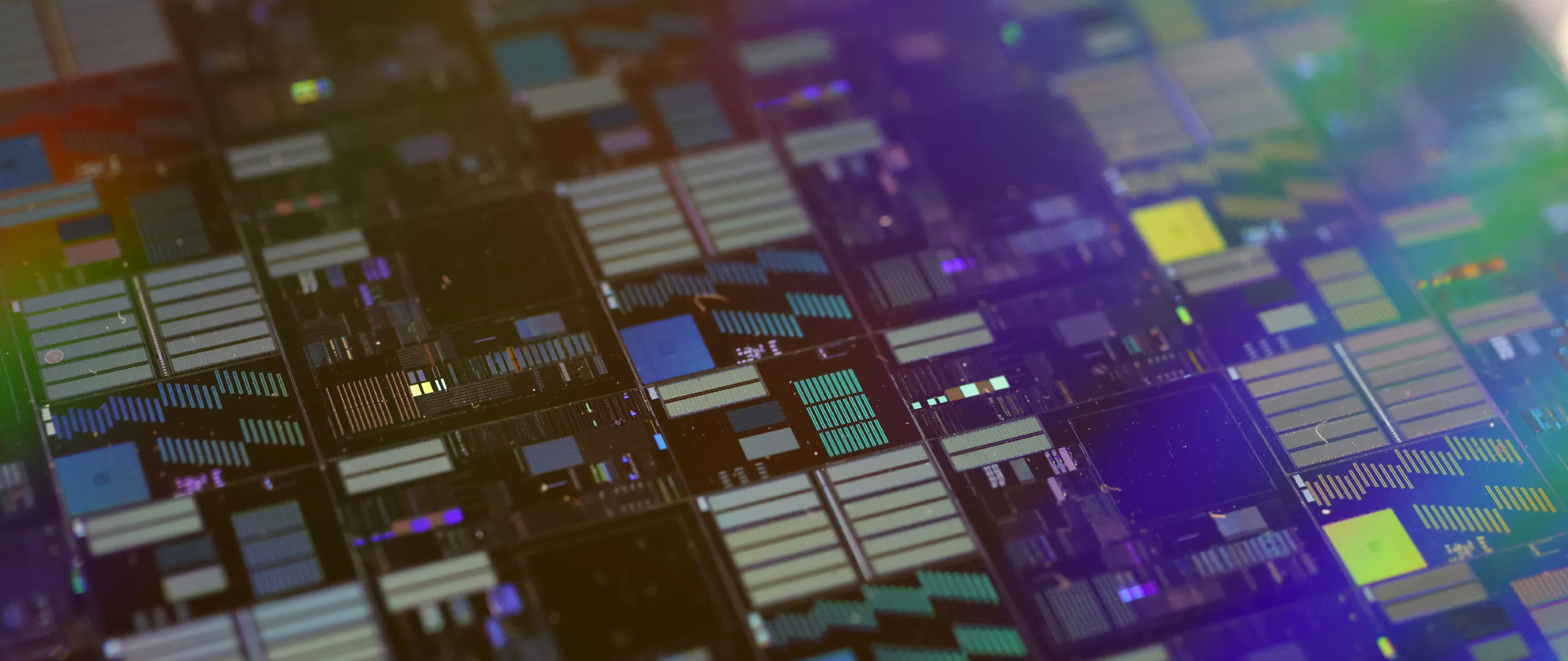
A 300 millimetre silicon wafer in the clean rooms at the Globalfoundries fabrication plant
(Image credit: Getty Images / Bloomberg)

All three leading-edge foundries — Intel Foundry, Samsung Foundry, and TSMC — have initiated mass production of chips using 2nm-class process technology. Samsung was the first one to start production using its SF2 node (though it could be argued that this is a rebadged SF3P) around mid-2025, Intel followed suit with its 18A node in November (albeit at development lines in Oregon, not production lines in Arizona), and TSMC initiated high-volume manufacturing using its N2 process at two volume fabs in Taiwan in December. We outline what's next for these three leading-edge foundries.

The current state of the market

Swipe to scroll horizontally

Row 0 - Cell 0

18A vs 3

18A vs 20A

18A-P vs 18A

14A vs 18A

14A-E vs 14A

Power

15% perf. per watt

10% perf. per watt

18%

25% - 35%

lower

Performance

15% perf. per watt

10% perf. per watt

9%

15% - 20%

higher

Density*

1.3X

slightly higher

-

1.3X

higher

Transistor

RibbonFET GAA

RibbonFET GAA

RibbonFET GAA

2nd Gen RibbonFET GAA

2nd Gen RibbonFET GAA

Power Delivery

PowerVia BSPDN

PowerVia BSPDN

PowerVia BSPDN

PowerDirect BSPDN

PowerDirect BSPDN

High Volume Manufacturing

H2 2025

H2 2025

2027 (?)

2028 (?)

2029 (?)

Swipe to scroll horizontally

Row 0 - Cell 0

A16 vs N2P

N2X vs N2P

N2U vs N2P

A14 vs N2

A13 vs A14

A12 vs A16

Power

-15% ~ -20%

lower

8% - 10%

-25% ~ -30%

?

lower

Performance

8% - 10%

10%

3% - 4%

10% - 15%

?

higher

Chip Density*

1.07x - 1.10x

?

?

1.2x

?

denser

Logic Density

?

?

1.02X - 1.03X

1.23x

1.06X

denser

Transistor

GAA

GAA

GAA

2nd Gen GAA

2nd Gen GAA

2nd Gen GAA

Power Delivery

SPR

Front-side w/ SHPMIM (?)

Front-side w/ SHPMIM (?)

Front-side w/ SHPMIM (?)

Front-side w/ SHPMIM (?)

SPR

High Volume Manufacturing

2027

2027

2027

2028

2029

2029

Anton Shilov is a contributing writer at Tom’s Hardware. Over the past couple of decades, he has covered everything from CPUs and GPUs to supercomputers and from modern process technologies and latest fab tools to high-tech industry trends.