


News |
By Asma Adhimi
CVD Equipment Corporation has demonstrated high-quality single-crystal silicon carbide (SiC) boule growth, marking a notable step forward in wide bandgap semiconductor manufacturing. The results come from a collaboration with Stony Brook University, where the material was characterized.
For eeNews Europe readers, this development is relevant as SiC continues to gain traction in power electronics, EVs, and high-efficiency energy systems. Improvements in crystal quality directly impact device performance, yield, and cost.
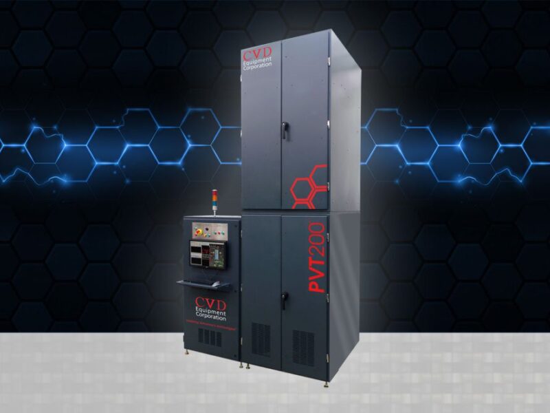
The SiC boules were grown using Physical Vapor Transport (PVT) systems developed by CVD Equipment Corporationand analyzed at the university’s onsemi Research Center for Wide Bandgap Materials. According to the analysis, the boule exhibited a 4H crystal structure, free of polytypes and with low defect density — key indicators of high material quality.
Such characteristics are critical for next-generation semiconductors, where defects can significantly degrade performance in high-voltage and high-temperature applications. The result strengthens CVD’s position in supplying advanced equipment for emerging semiconductor markets.
Michael Dudley, Professor and Director of the research center, stated: “Using the PVT systems developed by CVDE to successfully grow silicon carbide single crystal boules under the auspices of the onsemi center is a natural evolution of the long-term collaboration between CVDE and SBU. The synergy of the expertise at CVDE in PVT systems and the prolific research background in silicon carbide and other wide bandgap materials at SBU will propel the next generation of crystal growth technologies for silicon carbide and other wide bandgap semiconductor materials.”
The partnership highlights the growing importance of academia-industry collaboration in accelerating semiconductor innovation. Manny Lakios, CEO of CVD Equipment Corporation, added: “We are pleased with our collaboration with Stony Brook University which enables the opportunity to demonstrate the performance of our Physical Vapor Transport equipment and our commitment to enabling the next generation of silicon carbide technology.”
With demand for SiC devices rising across automotive and industrial sectors, advances in crystal growth technology are expected to play a central role in scaling production and improving device reliability.
 If you enjoyed this article, you will like the following ones: don't miss them by subscribing to :
此内容由惯性聚合(RSS阅读器)自动聚合整理,仅供阅读参考。 原文来自 — 版权归原作者所有。