


Lexar recently invited Tom’s Hardware, along with several other journalists, to visit its Shenzhen office, which sits north of Hong Kong, as well as its research and development facilities at Zhongshan across the bay. From there, the company took us to their Suzhou factory, about an hour and a half to the west of Shanghai, to explore their automotive storage production line.
The company is primarily known for its flash memory products, particularly for high-performance microSD, SD, and CFexpress cards for cameras and other portable devices, as well as flash drives and card readers. However, the company has recently been making a push towards modern SSDs and RAM modules, and it’s also working on the next generation of AI-ready storage solutions.
Article continues below
Moving beyond memory cards and flash drives
Lexar has continued producing removable storage solutions after its 2017 acquisition by Longsys. Just one year after the purchase, the brand was the first to commercially release a 1TB SD card. The company also claimed that it had the world’s fastest CFexpress Type B cards in 2022, which is crucial for both photographers shooting in burst mode and videographers shooting at high-resolution 4K video. Just last year, the company also released the world’s first stainless steel SD cards, featuring an IP68 environmental protection rating while also providing much more strength than regular plastic SD card models.
But now that Lexar was under the wing of Longsys, the company had access to formidable resources for research and development, as well as the nearly two decades of experience that its parent firm had in working with flash storage. Although the company had already been making USB flash drives before 2017, it was only after the Longsys purchase that the company started making and selling proper drives.
One of the first Lexar SSDs we’ve seen is the NM600 M.2 NVMe SSD, which, although it did not offer mind-bending performance, was an affordable and efficient SSD that offered a great solution for those looking for relatively affordable storage. Since then, Lexar has released several NVMe SSDs, like the NM790, which offered excellent sustained read and write speeds while staying power efficient and is priced competitively, especially at the 4TB capacity, as well as the 1TB Lexar Play M.2 2230 SSD, which is one of the best solutions for expanding storage on gaming handheld devices.
Image
1
of
2
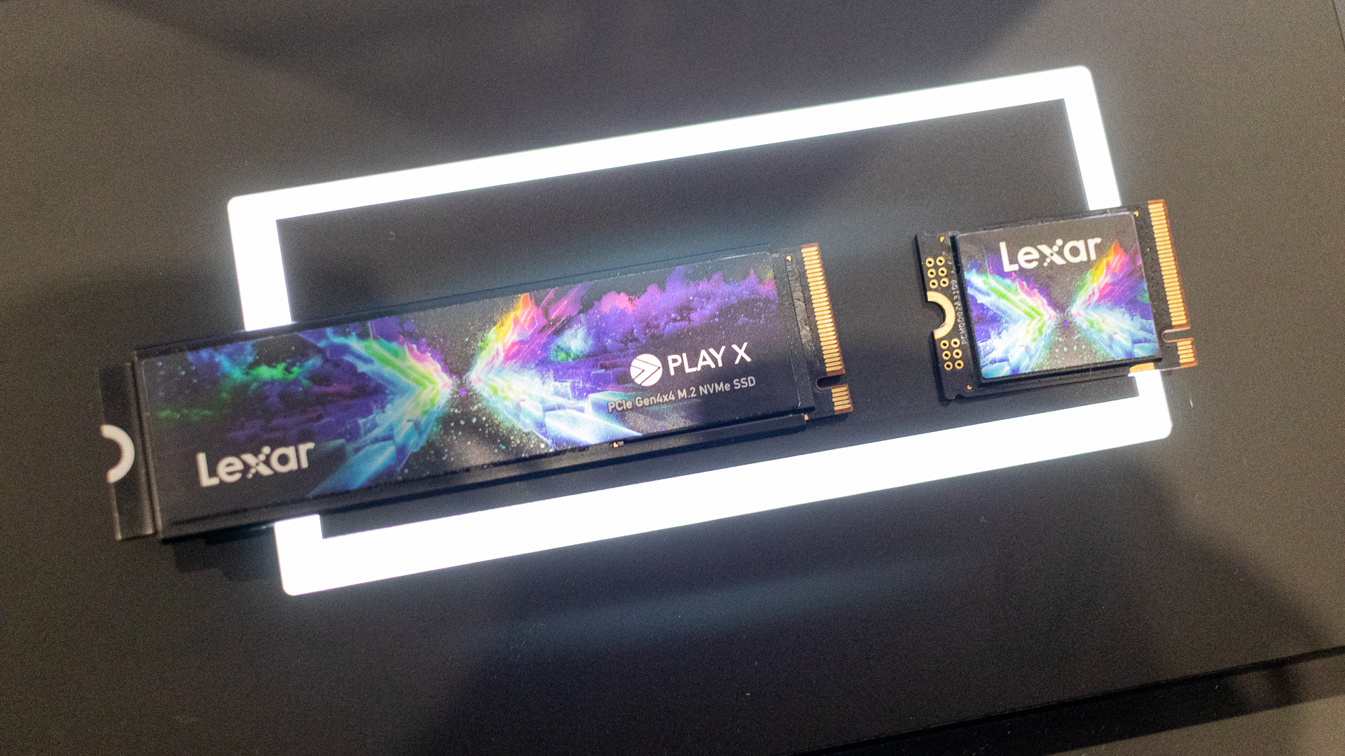
The company has also started building its own storage controllers, which manage how data is stored, moved, corrected, and retrieved from the NAND flash chips used by memory cards. This would allow Lexar to have more in-depth control of how its memory products would perform and differentiate its offerings from the competition. At the moment, Lexar’s Silver Plus microSD, Blue microSD, Silver Plus SD, and Silver SD cards already use in-house controllers.
Aside from building its own storage controllers and expanding into solid state drives, the company also ventured into RAM with its basic DDR4-2666 C19 memory modules in 2020 and the Hades gaming RAM the following year. By 2023, the company made the Ares RGB DDR5-6000 C34 gaming RAM, which supports both Intel XMP 3.0 and AMD EXPO.
Of course, Lexar also saw the need for specialized storage in the age of AI. Because of this, it’s planning to release its AI Storage Core solution, which is more than just a faster, more performant memory solution. Of course, these will have higher read and write speeds, which is crucial for the massive amounts of data that AI handles, but will also have better encryption to protect the sensitive data handled by AI models. Lexar also says that they’ll be more robust, especially for applications in AI-powered vehicles and robots, as well as having hot-swapping capabilities to make it more convenient to switch devices without requiring a reboot.

The company says that it will offer multiple configuration options for AI Storage Core devices, ensuring that manufacturers and end-users can pick one that’s optimized for their application. It’s also working with various AI vendors, ensuring that Lexar’s storage solutions will be supported in future AI applications, allowing for easier and direct access to the data stored within them. There’s also development of supporting snapshots directly on the storage device’s firmware, giving users a secure backup directly on the device and making it easier to restore their data in case something goes wrong during the AI workflow, making it easier to roll back to an earlier snapshot.
Of course, Lexar cannot achieve all its plans without putting in the effort to develop new technologies. So, the company invited us to explore their various sites to see what it’s doing to achieve its goal of “Bridging Continents and Powering the World.”

Research and development for next-generation storage technologies
One of the first places we visited was the Longsys Innovation Laboratory, located in the Foresee Building at Zhongshan. This is where Lexar’s parent company works on developing next-generation products, including DDR5 and LPDDR5/5X memory modules, PCIe 5.0 storage solutions, UFS4.1 memory cards, as well as CXL2.0/3.0 for data centers and AI systems. The lab covers an area of over 9,000 square feet and is staffed by over 50 personnel, of which 20 are full-time engineers, scientists, and researchers.
Everything begins at the Design Simulation & Signal Analysis Lab, where new Lexar products are developed, validated, and engineered. The Design Simulation Lab is where upcoming storage solutions are tested for thermal performance, structural rigidity, and signal and power integrity, while the Signal Analysis lab looks at the high-speed signals being sent throughout the entire system to ensure everything stays in spec and operates reliably.
Since Lexar relies on third-party suppliers for NAND and DRAM supplies, it must ensure the quality of the dies it receives and know exactly what’s inside each product it manufactures. This is where the Chip Resource Analysis Lab comes in, where multiple high-end machines test timings, memory redundancy, and the memory core, as well as running accelerated aging under stress (also known as burn-in testing), to ensure the quality and reliability of Lexar products over time.
Image
1
of
2
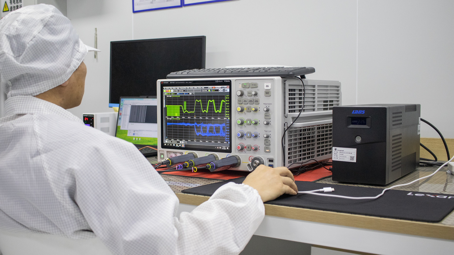
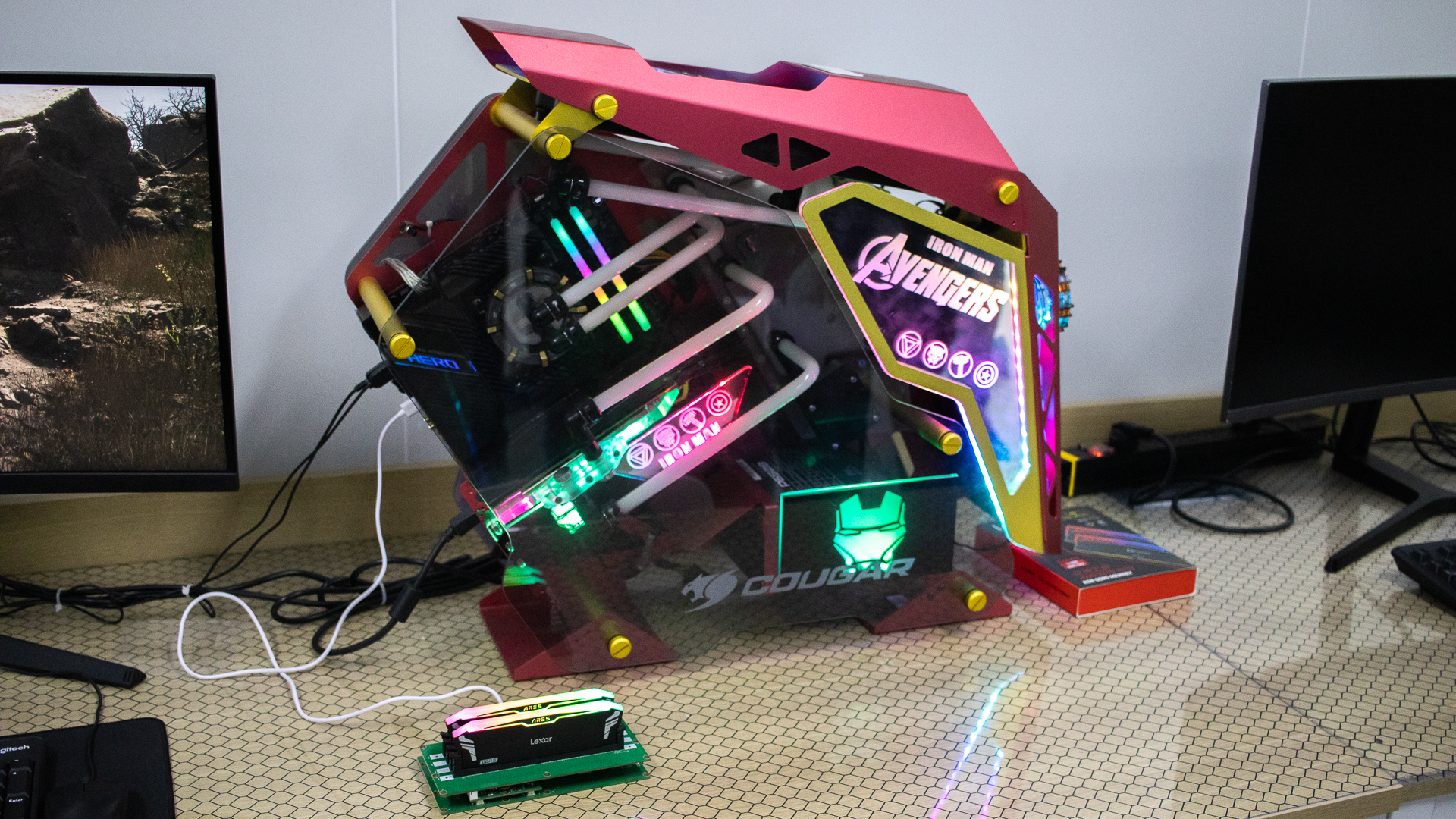
There are several labs that deal with completed products. There’s the System Verification Lab, where finished storage and memory items are tested for their power draw and timings, ensuring that Lexar DRAM meets JEDEC specifications. Lexar has a high-end gaming PC installed in the lab so that they can run their hardware on various benchmarking apps like AIDA64, 3DMark, and PCMark.
The Reliability Lab is where things are getting interesting, as Lexar puts its various products through their paces here. It has various testing machines, including the Drop Tester for simulating dropping an item from a height of up to 1.5 meters or 4 feet to a concrete or steel floor and the Roller Drop Tester, which continuously tumbles items between 5 to 25 RPM. There’s also the Plug-in/out Force Test machine, which simulates plugging in a memory card into a slot thousands of times and with various levels of force, the Tensile Test machine, which basically pulls on materials to see how much strength it takes to break them apart, and several other devices that check the durability of their prototypes and other products.
Aside from physical strength, the company also tests for electrostatic discharge resistance in its ESD lab, ensuring that its memory cards, storage drives, and memory modules aren’t killed by everyday static that people build up from their environment.
The tests we’ve mentioned above are mostly limited to day-to-day use. At the end of the hall sits the Environmental Lab, where Lexar puts its prototypes and products through the wringer. There are four testing machines here — the Salt Spray Test, which accelerates aging through a corrosive environment, the Precision High-Temperature Oven, where Lexar products are exposed to high temperatures while they are running, the Highly-Accelerated Stress Test, for reliability failure analysis, and the Dye Penetration Test, which looks at the effects of thermal shock on various components.
Image
1
of
3
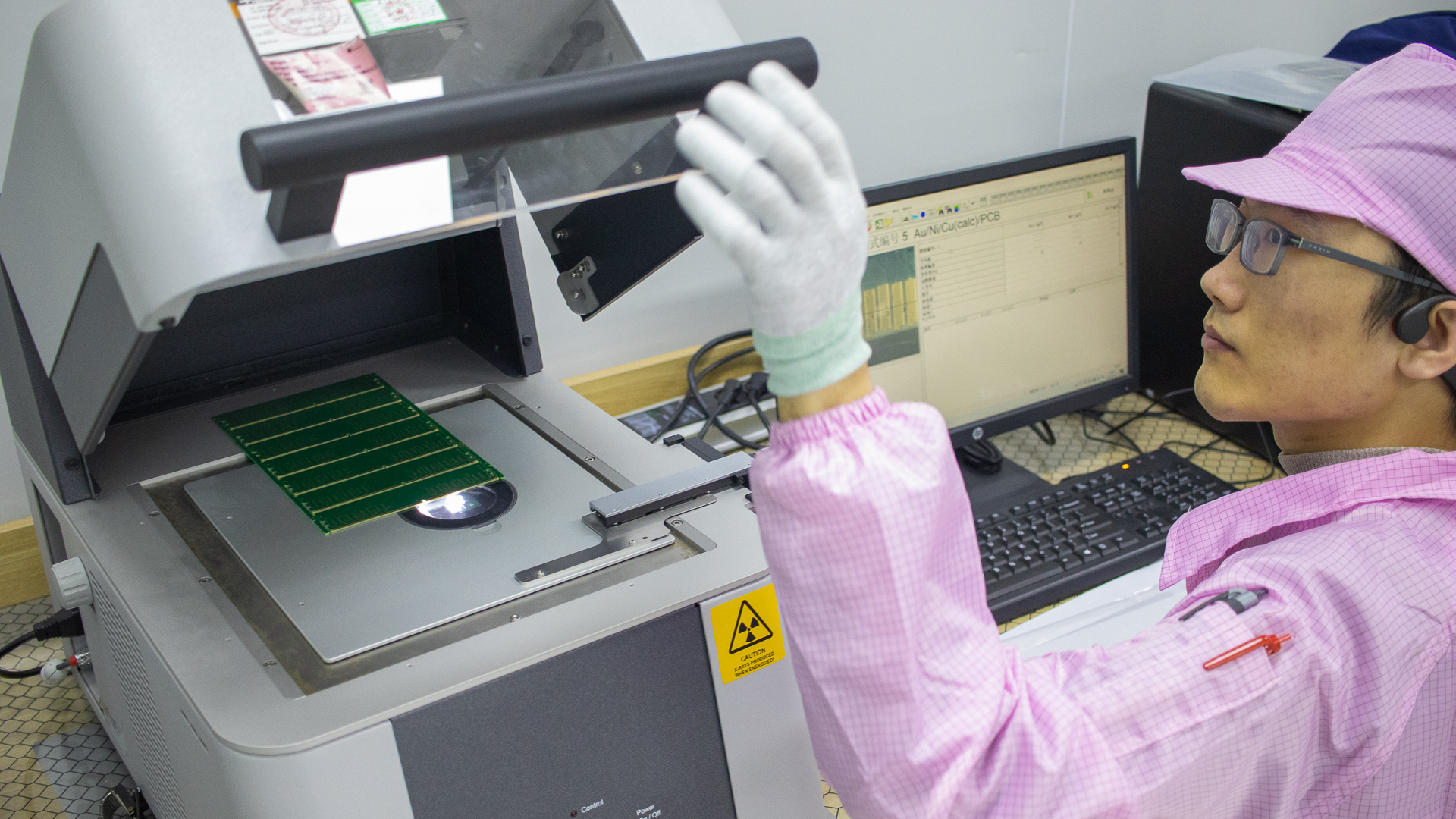
Besides the ESD Lab, you’d find the X-ray Lab, where the tiny wiring and connections in the chip are analyzed. Inside it, you’ll find a combined 2D X-Ray and CT Scan machine, allowing Lexar engineers to find minute, microscopic defects. There’s also the Failure Analysis Lab, which looks at how the items fail after this series of tests, allowing Lexar to figure out what went wrong with them and rectify their shortcomings, ensuring that they do not fail once out in the real world.
Last, but not least, we visited the Materials Analysis Labs, where the scientists and engineers visually inspect the chips. Note that they do not just place them under a microscope — instead, this is an involved process where they would put the memory or storage module they want to inspect in resin and then use a precision cutter machine to exactly slice the material and reveal the area where the suspected damage is.
Image
1
of
3
Now, all the testing here is done directly on the Lexar products and prototypes. However, storage and memory do not exist in a vacuum — instead, they must work with a massive number of different devices, like cameras, drones, security cameras, gaming handheld devices, desktops, laptops, tablets, dashcams, and so much more. So, our next stop was the Longsys Quality Labs.
An extensive compatibility testing lab
Lexar has an extensive portfolio of memory and storage products, including CFexpress cards, SD cards, microSD cards, the NM card for some Huawei phones, portable SSDs, USB flash drives, M.2 and SATA SSDs, DDR4 and DDR5 memory modules, card readers, enclosures, and more. If Lexar plans to release any new product, it must ensure that it will work across a wide range of devices already on the market. Because of this, Longsys Quality Labs keeps more than 1,200 different gadgets across 35 categories to ensure that it can test its products before release.
For example, we saw more than 30 handheld gaming consoles on one desk, featuring popular brands and models like the Steam Deck, ROG Ally X, Lenovo Legion Go, and the Nintendo Switch 2, as well as from more niche brands like OneX Player, Ambernic, and more. There are also several drones and action cameras from DJI, as well as shelves of DSLRs, mirrorless, and point-and-shoot cameras from Canon, Nikon, Sony, and Fujifilm. The Lexar team also had multiple phones, including those from Chinese brands like Huawei, Xiaomi, Vivo, and Oppo, as well as popular international brands such as iPhone and Samsung. Aside from these flash devices, other rooms also stored a ton of more mundane gadgets, like dashcams, security cameras, and even automotive modules.
Image
1
of
5
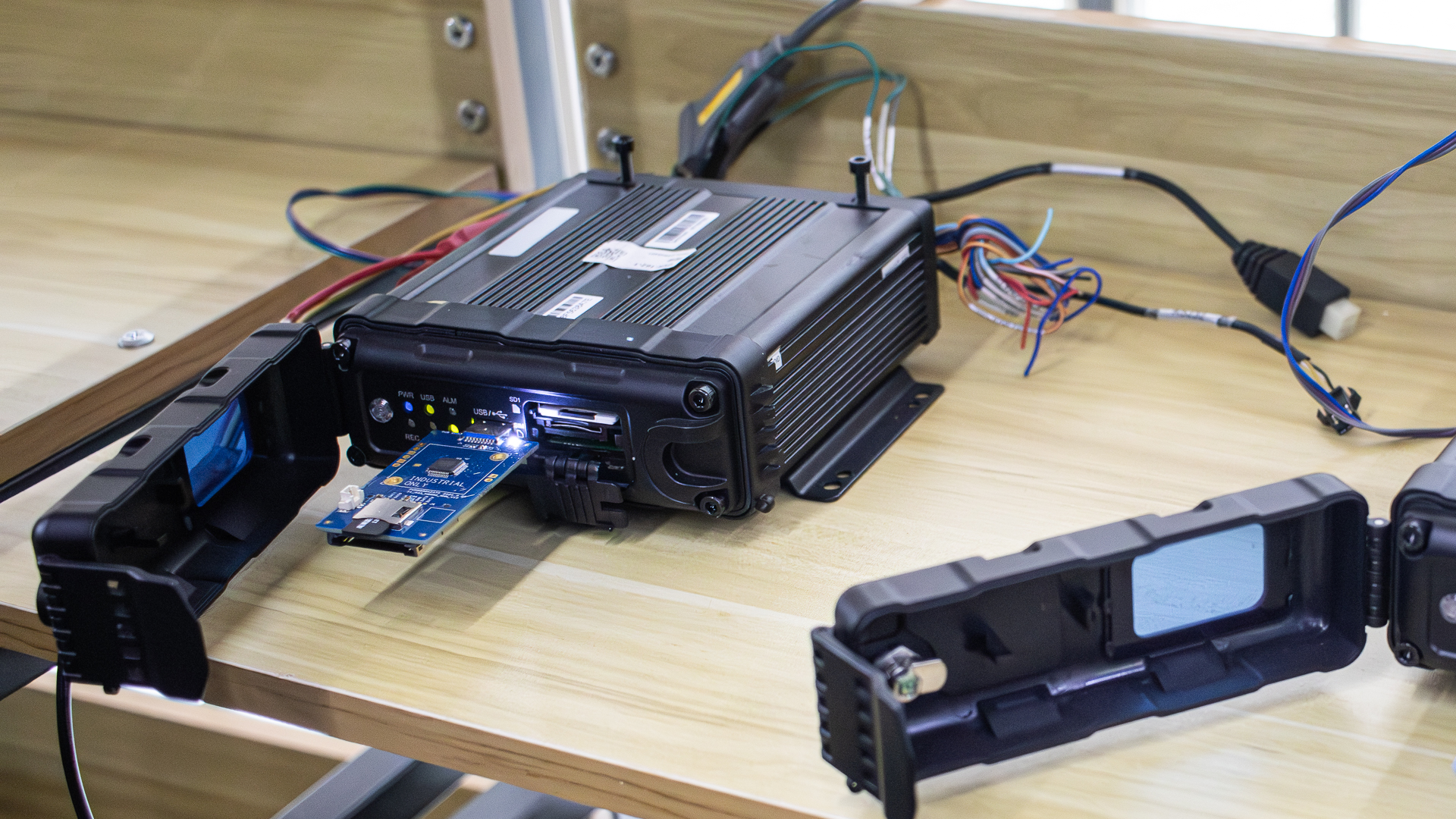
After exploring the lab, we visited the Memory History Museum, where Lexar showed how storage technologies developed from prehistoric knots to the SSDs that we know today. We ended our day there, as our next stop would be the company’s manufacturing base in Suzhou, a two-hour flight from Shenzhen, which we took the following day.
Exploring the Longforce automotive storage production facility
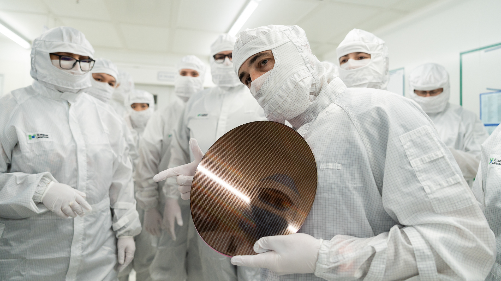
Our entire group landed in Shanghai, and we took a one-and-a-half-hour drive to the Longforce Technology (Suzhou) Co., Ltd., which is the company’s manufacturing arm. We then made our way to the company’s production line for automotive storage, where we saw how NAND silicon wafers are turned into automotive-grade storage solutions. Since this is a silicon production line, we all had to wear cleanroom suits and get blasted with air jets before entering the actual production area. That way, we minimize the chances of bringing in contaminants that would affect yield rates.
Image
1
of
2
The NAND arrives from the suppliers in wafer form, where it must first undergo taping, which is the mounting of the wafer to a backing material to ensure its rigidity during processing. That’s because a silicon wafer is extremely thin, and the backing material will protect it from cracking. From here, the wafer first undergoes pre-grinding, which thins out the wafer and makes it ready for cutting. It’s then cut into pieces with a laser using a technique called stealth dicing, because the cuts were made under the surface. From there, the wafer is finally fully ground to bring the wafer to its final thickness.
Once all of that is completed, the wafer is then finally mounted, and the tape is removed through DDS. It then goes through various processes until the die is mounted onto a substrate. From there, it will go through wire bonding, which connects all the layers of the die to the substrate, and be packaged via a C-Mold process. From there, it receives branding, and solder balls are attached to the underside of the substrate to make it ready for attachment to a PCB.
Image
1
of
3
Note that the process does not end there, as the chips are all built together into a single molded panel. They must first be cut into individual pieces through singulation. Once that is done, they go through final testing and quality control, and then the chips are packaged for delivery to clients.
Let's move to the executive Q and A on the following page.