










Researchers at the Korea Advanced Institute of Science and Technology (KAIST) have developed a technique to carve microscopic liquid-cooling channels directly inside silicon semiconductor chips.
Interestingly, the computer architecture slashed the energy required for cooling by pumping ordinary, room-temperature water straight through the chip’s internal structure.
“As the performance of AI semiconductors and advanced electronic packaging becomes increasingly limited by heat, we expect this technology to serve as a foundational cooling solution for future high-performance computing systems,” said Professor Sung Jin Kim.
The rapid advancement of high-performance AI chips has created a severe energy crisis for data centers, which require massive amounts of electricity both to power intensive computations and to cool down the resulting heat.
Typical cooling methods, such as roaring air fans and external copper heat spreaders, are reaching their physical limits. Hence, the industry is urgently looking for thermal alternatives.
To appreciate this development, you have to understand why standard liquid cooling is flagging.
Most modern liquid systems rely on an external “cold plate” pressed against the outside of a chip. The coolant has to travel from one end of the hardware to the other. This long trek creates immense fluid resistance.
It requires heavy-duty pumps pushing with massive pressure, which consumes a ton of energy. And at times, the fluid warms up along the way, leaving some parts of the processor chilled and others dangerously hot.
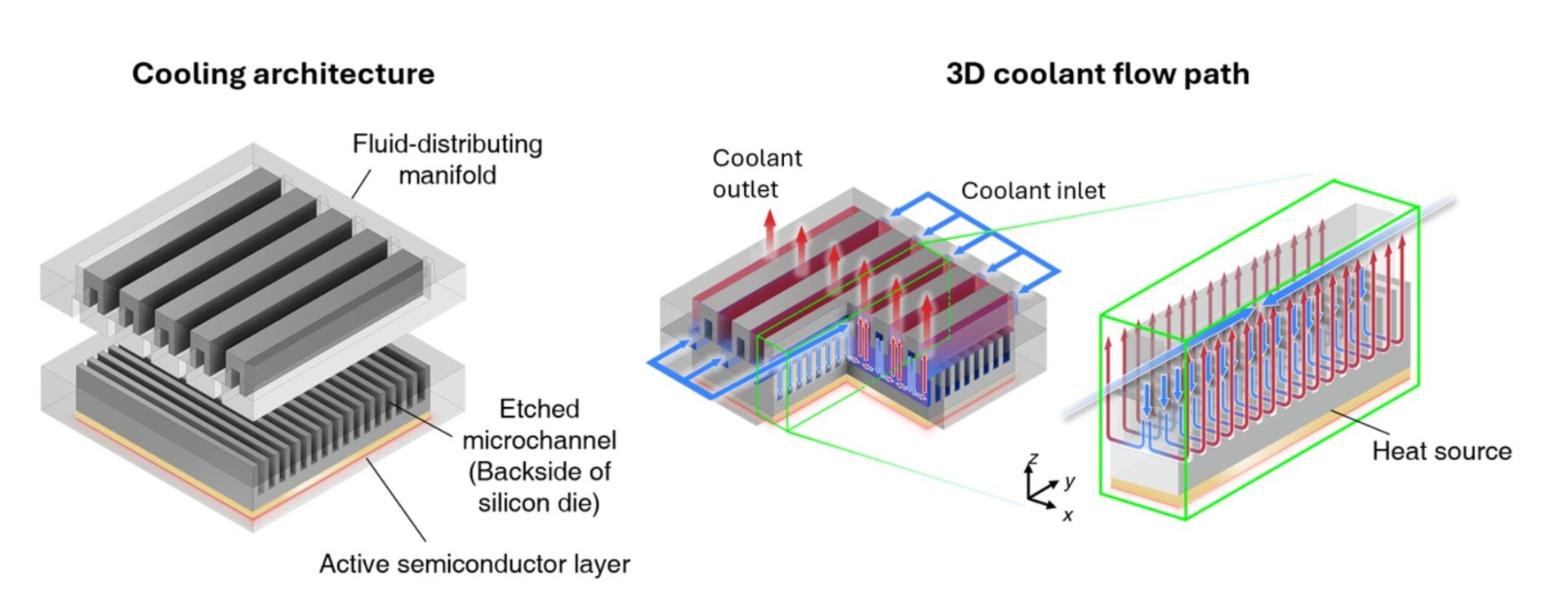
The KAIST team developed a liquid-cooling technology that cools semiconductors from the inside out. It uses ordinary room-temperature water to tackle high-heat-flux conditions at the source.
The design features multiple tiny inlets and outlets scattered uniformly across the chip.
The innovation centers on a “manifold microchannel” structure embedded directly inside the silicon, which mimics an efficient logistics network by using multiple strategic inlet and outlet points.
This decentralized design shortens the fluid’s travel distance, reducing flow resistance and pumping pressure. The researchers used a multi-fidelity optimization framework to perfectly balance channel dimensions and flow rates.
The KAIST team combined rapid 1D computational models with heavy-duty simulations to map an optimal, perfectly uniform flow. And the experimental results blew past expectations.
Notably, the system registered a cooling Coefficient of Performance (COP) of 106,000. That is an abstract engineering metric, but the context is historic: it is ten times higher than the previous world record published in Nature in 2020.
In plain terms, it means chip manufacturers need just one-tenth of the pumping power to remove the same amount of heat from a machine. Even under an extreme thermal load of 2,000 watts per square centimeter, the system kept the chip comfortably below 100°C (212°F).
Yet, the most disruptive detail of the experiment is how it’s made.
The researchers didn’t use exotic, hyper-expensive materials like synthetic diamond; instead, they used plain water. Furthermore, the entire fabrication process happens below 350°C (662°F).
It means the process is entirely compatible with existing commercial semiconductor manufacturing lines. Foundries can integrate this plumbing technique into current chip designs without buying billions of dollars in new machinery.
The development was published in the journal Energy Conversion and Management.
Mrigakshi is a science journalist who enjoys writing about space exploration, biology, and technological innovations. Her work has been featured in well-known publications including Nature India, Supercluster, The Weather Channel and Astronomy magazine. If you have pitches in mind, please do not hesitate to email her.
此内容由惯性聚合(RSS阅读器)自动聚合整理,仅供阅读参考。 原文来自 — 版权归原作者所有。