


惯性聚合 高效追踪和阅读你感兴趣的博客、新闻、科技资讯
阅读原文 在惯性聚合中打开

推荐订阅源

博客园_首页
Y
Y Combinator Blog
Engineering at Meta
Engineering at Meta
D
Docker
GbyAI
GbyAI
aimingoo的专栏
aimingoo的专栏
大猫的无限游戏
大猫的无限游戏
腾讯CDC
P
Proofpoint News Feed
A
About on SuperTechFans
WordPress大学
WordPress大学
Stack Overflow Blog
Stack Overflow Blog
Google DeepMind News
C
Check Point Blog
Microsoft Security Blog
H
Hackread – Cybersecurity News, Data Breaches, AI and More
L
LangChain Blog
MyScale Blog
MyScale Blog
博客园 - 三生石上(FineUI控件)
Hugging Face - Blog
Hugging Face - Blog
Microsoft Azure Blog
N
Netflix TechBlog - Medium
G
Google Developers Blog
OSCHINA 社区最新新闻
OSCHINA 社区最新新闻

Latest from Tom's Hardware in Tech-industry

Samsung engineer sentenced to 7 years in prison for selling chipmaking trade secrets to Chinese chipmaker — ex-employee supplied 10nm DRAM data to CXMT for $2 million Microsoft facing $2.8 billion UK lawsuit for overcharging 60,000 businesses using Microsoft Server on other clouds — Azure users allegedly received lower wholesale pricing Ransomware negotiator pleads guilty after leaking victims' insurance details to 'BlackCat' hackers — perp gave attackers a precise picture of exactly how much each target could afford to pay Congress moves to strip the DoC of chip-export discretion with the MATCH Act — DUV lithography machines among those targeted in chipmaking tool crackdown Anthropic's Model Context Protocol includes a critical remote code execution vulnerability — newly discovered exploit puts 200,000 AI servers at risk Iran claims US exploited networking equipment backdoors during strikes — says devices from Cisco and others failed despite blackout in attack that 'indicates deep sabotage' Cerebras files for IPO — company remains unprofitable despite 20x revenue growth Scientists solve decades-old 2D physics puzzle — Chaotic growth in a 2D quantum system obeys statistical laws Anthropic nuked a company's access to Claude, stopping 60 employees dead in their tracks — support via Google Form is the only recourse for vague usage policy violation Biohacker claims to have sequenced their own genome at the kitchen table with M3 Ultra Mac Studio, Claude, and a $3,200 sequencer — DIY project requires 100GB of data storage per run, oodles of RAM New Jersey datacenter expansion got $77m in tax breaks to create exactly one permanent job — JPMorgan's site already scored $35m and currently employs just 25 workers Chinese chipmakers made record profit in 2025, despite slipping margins — U.S shipments fall 34% as Beijing shores up local chipmaking efforts AI cloud company Vercel breached after employee grants AI tool unrestricted access to Google Workspace — hacker… Every SK hynix employee could receive $477,000 bonuses this year, almost $900,000 next year — 35,000 workers reportedly set to benefit from share of $169 billion projected operating profit US gov't blocks China's largest LED chipmaker's $239 million bid to acquire Dutch lighting firm Lumileds… Tokyo court rules movie and anime 'spoiler articles' are copyright infringement in landmark criminal case — detailed, monetized plot summaries land man in Japanese prison Voyager 1 gets emergency instrument shutdown to solve escalating power crisis and give it ‘about a year of breathing room’ — interstellar spacecraft's nuclear power source is dying, leading to intensifying countermeasures Russian-made Shahed drones are ‘disintegrating in the air before reaching their targets’ due to shoddy manufacturing, video shows — commentators call Russian clones of Iran's drones 'flying garbage' Inventor showcases 3D printer filament dryer that mines Bitcoins and dries filament with waste heat, capable of 6 TH/s at 140W — joins Bitcoin-mining 3D printer in hobbyist-focused miner lineup Bluetooth tracker hidden in a postcard and mailed to a warship exposed its location — $5 gadget put a $585 million… Techie buys fake Ledger Nano S+ hardware crypto wallet and almost falls for phishing — a convincing clone would… Nvidia CEO Jensen Huang ‘nearly lost his composure’ when pressed on selling chips to China — ‘You’re not talking to someone who woke up a loser’ US lawmakers amend new restrictions on Chinese chipmakers — MATCH Act Analytics group signals possible delays at 40% of AI data center construction sites — companies deny schedule holdups, but satellite imagery indicates otherwise Local political revolts threaten to derail US data center projects — mounting delays are already costing AI hyperscalers billions Intel hires tenured Samsung exec to lead Foundry Services — signals company focus on winning business from potential Foundry suitors Elon Musk pushing forward with Terafab at TSMC ups revenue guidance and CapEx, buoyed by Google and Pentagon in talks to run custom AI chips inside classified environments — Google pushes for tight controls for TPUs surrounding use for mass surveillance and autonomous weapons TSMC warns of Intel Foundry
NEO Semiconductor's revolutionary 3D X-DRAM for AI proces...
Etiido Uko · 2026-04-24 · via Latest from Tom's Hardware in Tech-industry
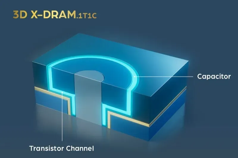
NEO Semiconductor 3D X-DRAM
NEO Semiconductor 3D X-DRAM (Image credit: NEO Semiconductor)

NEO Semiconductor announced on April 23rd that its 3D X-DRAM technology has successfully passed proof-of-concept (POC) validation, demonstrating that a new class of high-density DRAM can be manufactured using existing 3D NAND infrastructure. The company simultaneously announced a new strategic investment led by Stan Shih, founder and former Chairman and CEO of Acer, and a board director of TSMC for over two decades.

At the center of the announcement is the company’s 3D X-DRAM technology, a new class of DRAM that aims to break past conventional memory scaling limits by adopting a vertically stacked architecture designed for higher density, lower power consumption, and improved suitability for AI-driven workloads.

Article continues below

The proof-of-concept chips, fabricated and tested at Taiwan's National Institutes of Applied Research - Taiwan Semiconductor Research Institute (NIAR-TSRI) in collaboration with National Yang Ming Chiao Tung University, delivered the following results:

Read/write latency: under 10 nanoseconds
Data retention: over 1 second at 85°C/185°F (claimed 15× improvement over JEDEC standard)
Bit-line disturbance: over 1 second at 85°C (185°F)
Word-line disturbance: over 1 second at 85°C
Endurance: greater than 10¹⁴ cycles

Industry commentary included in the announcement was quite positive — although this does not imply confirmation of viability at scale. TechInsights’ Jeongdong Choe described the results as a “significant milestone” in the shift toward 3D memory architectures, noting that conventional DRAM scaling is approaching physical limits and that the industry is increasingly exploring vertical alternatives.
Chips

(Image credit: Shutterstock)

The broader context behind this development is the growing strain AI workloads are placing on memory systems. While GPU compute performance has scaled aggressively over the past decade, memory bandwidth — the rate at which data can be fed to those processors — has become a limiting factor in large-scale AI training and inference systems. This has already driven widespread adoption of high-bandwidth memory (HBM), a vertically stacked DRAM architecture integrated close to GPUs. However, HBM presents complex 3D stacking and bonding requirements and high manufacturing costs.

Get Tom's Hardware's best news and in-depth reviews, straight to your inbox.

Quick clarification sidebar: 3D X-DRAM and HBM both use vertical stacking concepts, but they stack different things in different ways. HBM stacks multiple finished DRAM dies on top of each other, then connects them with through-silicon vias (TSVs) and places them beside/near a GPU or CPU on an interposer. 3D X-DRAM, based on NEO’s claims. aims to build memory cells in a 3D NAND-like monolithic vertical structure, where layers are fabricated as part of the memory array itself rather than stacking separate packaged DRAM dies.

3D X-DRAM is just one of several technologies under development to address the AI memory problem. Just a day before NEO Semiconductor’s announcement, we reported that SAIMEMORY and its ZAM architecture, backed by SoftBank and Intel with Japanese government support, is pursuing a similar goal on a parallel track.

NEO Semiconductor’s device successfully passed extensive electrical and reliability evaluations, confirming the robustness and stability of the proposed memory architecture. It is important to reiterate that this is a proof of concept, not a production-ready memory chip. The road from validated POC to commercial volume is long — and littered with the remains of promising memory technologies that never made it out of the lab. However, with NEO Semiconductor's usage of established 3D NAND processes, the future is bright.

"The successful proof-of-concept not only demonstrates the potential of innovative memory architectures, but also confirms the feasibility of implementing advanced memory technologies using mature processes. This collaboration among NEO, NYCU IAIS, and NIAR-TSRI further underscores the value of industry–academia partnerships in accelerating innovation from concept to practical implementation," said Jack Sun, Senior Vice President of NYCU and Dean of IAIS, and former CTO of TSMC

Google Preferred Source

Follow Tom's Hardware on Google News, or add us as a preferred source, to get our latest news, analysis, & reviews in your feeds.

Etiido Uko is an engineer and technical writer with over nine years of experience in documentation and reporting. He is deeply passionate about all things gadgets, technology, and engineering.