
惯性聚合 高效追踪和阅读你感兴趣的博客、新闻、科技资讯
阅读原文 在惯性聚合中打开

推荐订阅源

人人都是产品经理
人人都是产品经理
Google DeepMind News
博客园 - 【当耐特】
量子位
博客园 - 司徒正美
爱范儿
爱范儿
Hugging Face - Blog
Hugging Face - Blog
博客园 - 聂微东
Jina AI
Jina AI
J
Java Code Geeks
腾讯CDC
大猫的无限游戏
大猫的无限游戏
V
Visual Studio Blog
I
InfoQ
D
Docker
Recent Announcements
MongoDB | Blog
MongoDB | Blog
博客园 - Franky
宝玉的分享
宝玉的分享
G
Google Developers Blog
GbyAI
GbyAI
Y
Y Combinator Blog
有赞技术团队
有赞技术团队
H
Help Net Security

Latest from Tom's Hardware in News-analysis

Kimi K3 rocks the AI industry as Moonshot AI undercuts closed-source American competitors on price — but the huge 2.8T open-weight model still needs serious hardware to deploy at scale Tower Semiconductor revives shuttered Panasonic-era fab in $3 billion Japan photonics expansion — METI-backed plan targets $3.6 billion revenue by 2028 Intel Intel Micron commits $500 million to GlobalWafers Anthropic says it can read Claude Elon Musk receives FTC greenlight to buy Mesh Optical as interconnects emerge as AI SiPearl South Korea Inside the history of DRAM price-fixing lawsuits — how HBM allocations could make a difference after two decades of failed cases U.S. PC shipments drop 7%, market isn Chinese Z.ai The AI tokenmaxxing party is crashing over spiraling costs — leaked consulting firm audio suggests no one is sure how to measure AI effectiveness US Secures Netherlands for Pax Silica Alliance in key win for strategic chip alliance — tension remains over MATCH Act restrictions Arm servers capture over 45% of data center market revenue — GPU clusters and high-end AI infrastructure fuel a tectonic shift away from x86 Post-silicon era gets closer as industry giants crack the 2D transistor scaling bottleneck with breakthrough tech — imec, ASML, and TSMC fab complementary 2D-material transistors at 50nm pitch on a 300mm wafer US pulls the Marvell details vision of optically-interconnected data centers spanning across thousands of kilometers — new interconnects sampling later this year would allow CSPs to pool resources based on workload Nvidia's high-speed AI data center storage servers break cover, touting 2.9 petabytes of storage and extreme PCIe 6.0 performance — Wiwynn shows off SCADA server with GPU-accelerated storage AI is set to consume up to 600 billion gallons of water by 2030 — rising energy consumption primarily to blame as… Google reportedly books Intel for packaging more than 3 million TPUs in 2028 — SK hynix is testing Intel's… Anthropic's warning over AI self-improvement has a hidden message — accelerating development requires more compute before companies ever risk losing control of frontier AI models Executives are cutting jobs for an AI future that hasn't fully arrived yet, even as productivity gains remain difficult to prove — data neither confirms nor refutes an AI unemployment apocalypse Jensen Huang says 'every edge device will become autonomous' — Nvidia maps one computing pattern from… AMD's Helios MI455X AI platform breaks cover, initial systems use UALink-over-Ethernet interconnects — AMD's Vera Rubin rival surfaces, but the downsides of Ethernet could hamstring performance Frore shows off LiquidJet Nexus coldplate for Nvidia Vera Rubin, other AI accelerators — offers up claimed 10% token generation boost over rival liquid-cooling solutions The rise of local agentic computing faces a brutal reality: rising DRAM prices —  RTX Spark, Gorgon Halo chips subject to 63% DRAM contract price hike this quarter Astera Labs showcases 320-lane PCIe 6.0 switch for vendor-agnostic scaling in data centers — up to 80 accelerators… AI costs begin to bite as agents may increase token demand by 24 times, says Goldman Sachs report — Uber and Microsoft among companies feeling the bite of tokenized billing IBM spins off America's first quantum chip foundry with $2 billion in federal and private funding — newly-minted 'Anderon' foundry to offer 300mm quantum wafer fab and manufacturing services
Japanese chemical giant JSR expands to Taiwan for EUV pho...
Luke James · 2026-05-13 · via Latest from Tom's Hardware in News-analysis
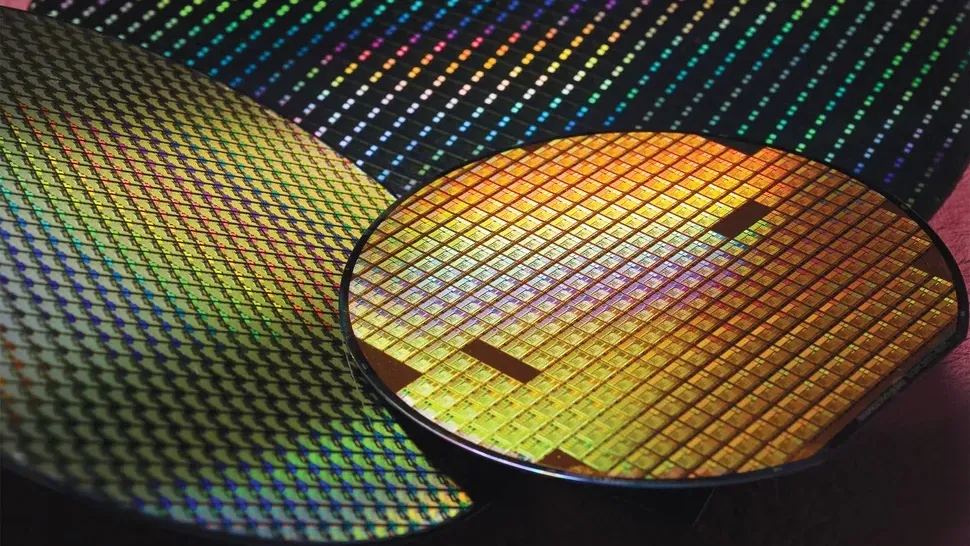
TSMC wafer
(Image credit: TSMC)

As chipmakers push EUV lithography toward its physical limits at 2nm and below, the advanced chemicals used to pattern those circuits have become a critical bottleneck. Photoresists, the light-sensitive materials that transfer circuit designs onto silicon wafers, must be reformulated for each new process node, and the most advanced EUV-grade resists are produced almost exclusively by a handful of Japanese suppliers. With AI chip demand driving record orders at leading foundries, those suppliers are now racing to build production capacity closer to their biggest customers.

JSR, the Japanese chemical maker that holds roughly a quarter of the global photoresist market, established a joint venture with Taiwanese partners Wah Lee Industrial and LCY Chemical in early April to build its first photoresist production facility in Taiwan. The plant, located in Yunlin County, is expected to come online as early as 2028 and will co-develop advanced photoresists with TSMC, ending the company's status as the last of Japan's three leading EUV-class resist suppliers without a Taiwanese manufacturing base.

Luke James is a freelance writer and journalist.  Although his background is in legal, he has a personal interest in all things tech, especially hardware and microelectronics, and anything regulatory.