
惯性聚合 高效追踪和阅读你感兴趣的博客、新闻、科技资讯
阅读原文 在惯性聚合中打开

推荐订阅源

J
Java Code Geeks
F
Fortinet All Blogs
云风的 BLOG
云风的 BLOG
MyScale Blog
MyScale Blog
D
DataBreaches.Net
Stack Overflow Blog
Stack Overflow Blog
A
About on SuperTechFans
Google DeepMind News
Microsoft Security Blog
腾讯CDC
The GitHub Blog
The GitHub Blog
Jina AI
Jina AI
B
Blog RSS Feed
I
InfoQ
N
Netflix TechBlog - Medium
T
The Blog of Author Tim Ferriss
Microsoft Azure Blog
Recent Announcements
GbyAI
GbyAI
H
Help Net Security
L
LangChain Blog
M
MIT News - Artificial intelligence
Y
Y Combinator Blog
aimingoo的专栏
aimingoo的专栏

THP Feed -- all premium articles

Intel Micron commits $500 million to GlobalWafers Anthropic says it can read Claude While the U.S. flip-flops on chip sanctions, China is building its own chip supply market — export controls are creating conditions for a Sino-Russian chip trade alliance Elon Musk receives FTC greenlight to buy Mesh Optical as interconnects emerge as AI Rapidus fab roadmap examined — first new leading-edge chipmaker in decades has one Hokkaido fab, a 2027 deadline, and 60 potential customers SiPearl South Korea Nvidia and Intel tout homegrown American chip supply chain prowess as country bolsters local production, but gaps remain — crucial Blackwell packaging steps remain offshore as projects grow in scope and scale Steam Machine interview full transcript: Valve engineers discuss $1,049 pricing, compact design, component shortages, and Windows support Inside the history of DRAM price-fixing lawsuits — how HBM allocations could make a difference after two decades of failed cases U.S. PC shipments drop 7%, market isn The bifurcated laptop landscape of Computex 2026 – MacBook Neo competitors with 8GB of RAM, and expensive Nvidia laptops promising an agentic-focused future of Windows on Arm Chinese Z.ai Imec Solidigm VP talks PCIe 6.0 SSDs, next-gen floating gate NAND, liquid cooled storage and more — Avi Shetty, VP of AI, Solutions & Market Enablement discusses the future of enterprise storage tech The AI tokenmaxxing party is crashing over spiraling costs — leaked consulting firm audio suggests no one is sure how to measure AI effectiveness US Secures Netherlands for Pax Silica Alliance in key win for strategic chip alliance — tension remains over MATCH Act restrictions China tops the list of fastest supercomputers with a CPU-only behemoth, ending US champion El Capitan Arm servers capture over 45% of data center market revenue — GPU clusters and high-end AI infrastructure fuel a tectonic shift away from x86 Ditching the cloud for local AI — how I use two mini PCs to process millions of tokens a day and save money on costly API fees Intel US pulls the Intel AMD’s massive SP7 socket for EPYC Venice and Intel’s gargantuan 9,324-pin socket for Diamond Rapids appear at Computex — SP7 and LGA9324-1 sockets will power the next generation of AI servers Marvell details vision of optically-interconnected data centers spanning across thousands of kilometers — new interconnects sampling later this year would allow CSPs to pool resources based on workload Nvidia's high-speed AI data center storage servers break cover, touting 2.9 petabytes of storage and extreme PCIe 6.0 performance — Wiwynn shows off SCADA server with GPU-accelerated storage AI is set to consume up to 600 billion gallons of water by 2030 — rising energy consumption primarily to blame as… Google reportedly books Intel for packaging more than 3 million TPUs in 2028 — SK hynix is testing Intel's… Analyzing TSMC's fab expansion roadmap — multi-fab N2 ramp, CoWoS, SoIC, and uncorking bottlenecks
Post-silicon era gets closer as industry giants crack the...
https://www.tomshardware.com/author/luke-james · 2026-06-19 · via THP Feed -- all premium articles
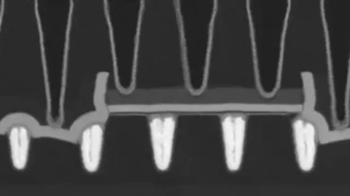
300mm integration of 2D-material transistors
(Image credit: imec/ASML/TSMC)

Imec, ASML, and TSMC have integrated both n-type and p-type transistors with atomically thin 2D channels on a single 300mm wafer at a 50nm contacted poly pitch, the tightest pitch demonstrated to date for complementary 2D devices and one that lands within range of leading-edge silicon.

The trio presented the work this week at the IEEE/JSAP Symposium on VLSI Technology and Circuits, using a single EUV exposure to print channel lengths as short as 28nm. Imec reported that 94% of the integrated transistors switched correctly, with an on/off current ratio above 100,000. The n-channel devices use molybdenum disulfide (MoS2), while the p-channel devices use tungsten diselenide (WSe2) or tungsten disulfide (WS2).

Luke James is a freelance writer and journalist.  Although his background is in legal, he has a personal interest in all things tech, especially hardware and microelectronics, and anything regulatory.