





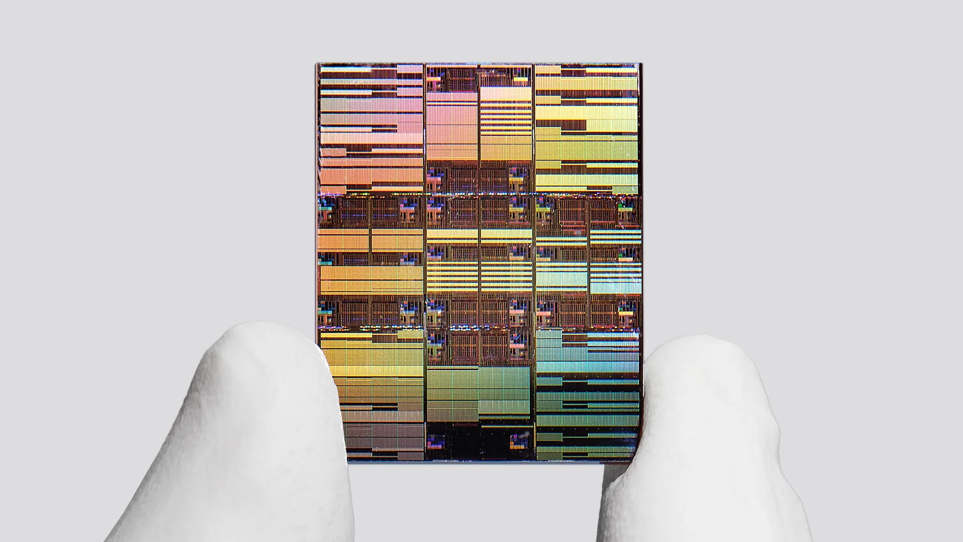
IBM on Thursday said it has produced the first test chip using its 0.7nm-class (7 angstroms) fabrication technology, the industry's first sub-1nm manufacturing process. The concept process technology relies on the so-called nanostack transistors and promises rather dramatic power, performance, and area (PPA) gains compared to IBM's 2nm-class node. To produce nanostack transistors, IBM uses two wafers instead of one, along with ultra-thin dielectric bonding, an arrangement that has never been used before.
IBM's 7A-class (or 0.7nm-class) fabrication process based on nanostack transistors is said to offer up to 50% higher performance and 70% higher energy efficiency compared to IBM's 2nm-class node based on nanosheet gate-all-around transistors the company introduced in 2021. Perhaps more importantly, IBM's nanosheet architecture provides a 40% higher SRAM density and even higher density improvements for logic transistors, gains that are extremely hard to achieve these days.
Such massive gains have been enabled by numerous innovations, but the key enabler is IBM's nanostack transistor architecture, which conceptually resembles CFETs and stems from GAA nanosheet transistors.
Two wafers instead of one
In modern process technologies, all logic transistors live in one active device tier, and NFETs and PFETs sit side by side laterally in the standard-cell layout. Nanosheet GAA transistors feature a more advanced internal geometry, but they still reside in this single-transistor tier, which gets harder to shrink with every generation.
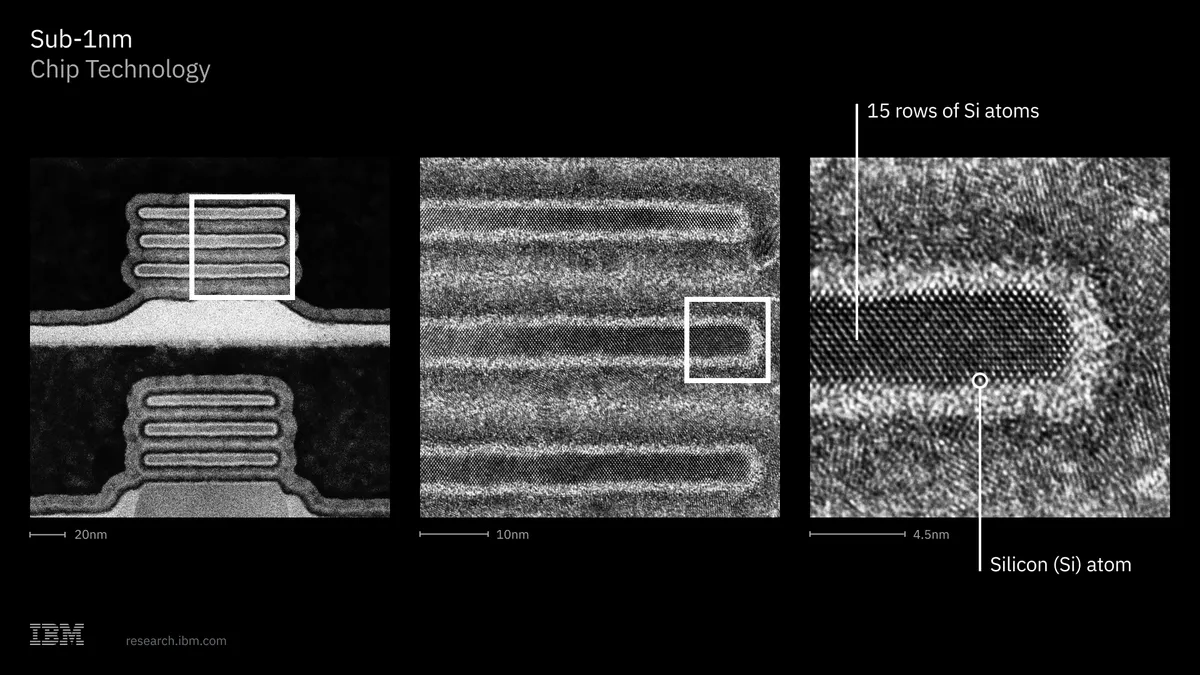
IBM's nanostack concept seems to separate complementary n-type and p-type transistors into vertically bonded tiers instead of placing them side by side in a single transistor layer. The payoff is a major reduction in the lateral footprint of a CMOS pair, as the architecture effectively turns one NFET+PFET structure from a 2D layout into a 3D stacked layout, which is why IBM can claim roughly double transistor density versus its 2nm research node without relying on conventional planar shrink.
While conceptually IBM's nanostack transistors resemble CFETs, the way IBM builds its nanostacks is fundamentally different compared to monolithic CFETs proposed by various chipmakers and organizations. N-type and p-type transistors are fundamentally the same kind of transistor used as complementary partners in CMOS logic, but they differ in carrier type (electrons for n-type and electron holes for p-type), switching polarity, and electrical behavior, which is why advanced process technologies tend to optimize them separately. However, these n-type and p-type transistors are made on the same wafer using essentially the same materials, so the level of their optimization is limited today.

Instead of building n-type and p-type transistors on the same wafer using the same materials, IBM builds them separately on different wafers and integrates them together using ultra-thin dielectric bonding in CMOS integration. This enables the company to optimize n and p-type channels independently, as each tier now can use different process conditions, different channel materials, different strain engineering, or even different geometries (though images from IBM indicate that the geometry of different transistors is the same).
As we see with all new process nodes, the nanometer-scale measurement doesn't coorelate to the physical dimensions of the device, but this remains a tremendous achievement.
Numerous caveats
Using two wafers for active transistor tiers instead of one could let IBM stack NFETs and PFETs vertically and optimize them independently, but such a method comes with a number of caveats that do not exist today with single-tier logic nodes.
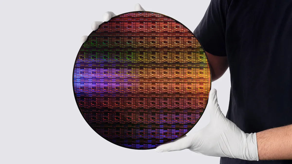
The biggest issues are alignment and bonding yield, because two advanced logic wafers must line up with extreme precision, and any defect at the bond interface can kill the stack. Secondly, routing and power delivery could get more complex with two active device tiers. Thirdly, cooling gets harder now that one active tier sits farther from the heat sink. Last but not least are the costs. IBM has to pay for two advanced FEOL wafers, additional bonding and thinning steps, and manage higher process complexity and likely lower yields. As a result, the whole concept only makes sense if the density, SRAM, and performance-per-watt gains are large enough to offset manufacturing difficulties and cost penalty. IBM says nothing about costs and manufacturability, and the test chip it has completed is the size of a fingernail,' so not hard to make by today's standards. Meanwhile, it is highly likely that the approach only makes sense for heavy-duty data center AI solutions (which are near reticle size) and not for mainstream processors for client applications. For others, monolithic CFETs can do the job.
On the bright side, IBM's 7A-class fabrication process does not rely on High-NA EUV lithography, as there are simply no such tools at the semiconductor research facility in Albany, New York, where IBM develops its technologies. Usage of proven Low-NA EUV systems makes it easier to get high yields now. Meanwhile, it remains to be seen how IBM's dual wafer approach works with High-NA EUV scanners that have half the exposure field compared to Low-NA EUV machines and therefore require field stitching, which does not really help yields. IBM implies that its next-generation nodes will use High-NA EUV lithography, so the company probably has ideas how to wed these new tools with its approaches to transistor designs.
In production in the next five years
When dealing with IBM's manufacturing technologies, one has to keep in mind that these are not fabrication processes that can be licensed and rapidly deployed at a high-volume fab, but are essentially a set of pre-competitive IPs, patents, and some R&D know-how that can be used to design an actual production node. For example, Rapidus licensed IBM's 2nm-class process, though it has yet to prove that it can create a competitive high-volume node.
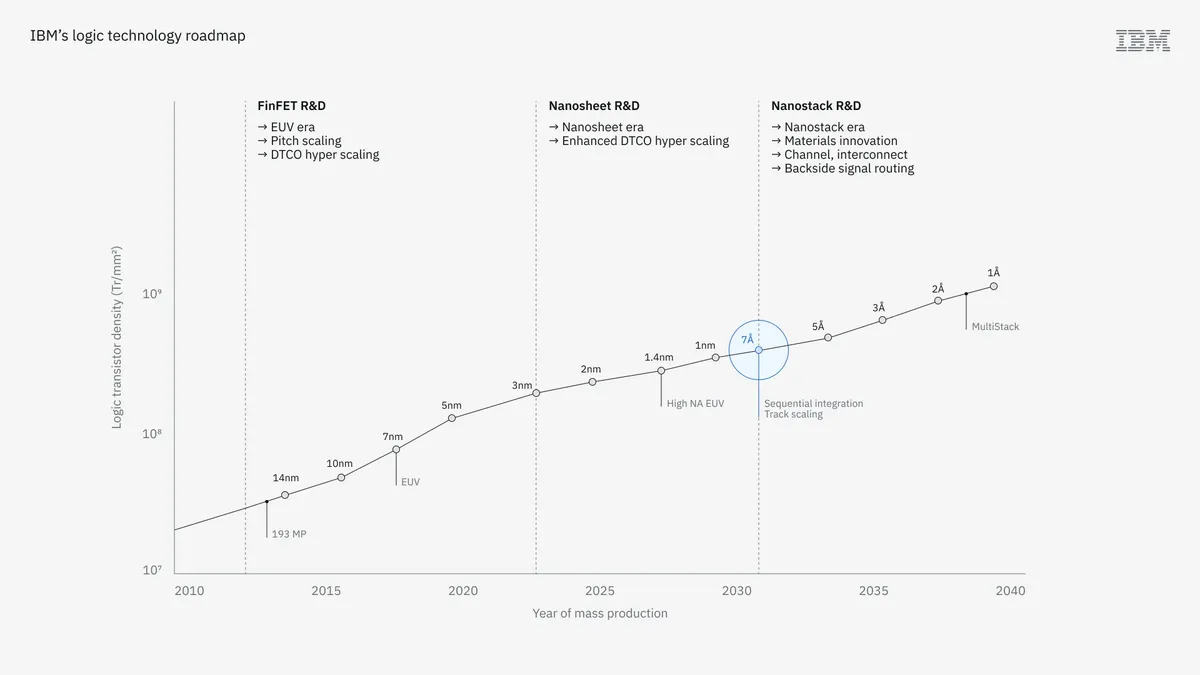
IBM believes nanostack could make sense for sub-1nm generations and potentially enter mass production within the next five years.

Follow Tom's Hardware on Google News, or add us as a preferred source, to get our latest news, analysis, & reviews in your feeds.