



惯性聚合 高效追踪和阅读你感兴趣的博客、新闻、科技资讯
阅读原文 在惯性聚合中打开

推荐订阅源

博客园 - Franky
云风的 BLOG
云风的 BLOG
人人都是产品经理
人人都是产品经理
博客园 - 叶小钗
Engineering at Meta
Engineering at Meta
Vercel News
Vercel News
Y
Y Combinator Blog
B
Blog
Microsoft Azure Blog
C
Check Point Blog
M
MIT News - Artificial intelligence
Jina AI
Jina AI
Cyber Security Advisories - MS-ISAC
Apple Machine Learning Research
Hugging Face - Blog
Hugging Face - Blog
阮一峰的网络日志
阮一峰的网络日志
罗磊的独立博客
Stack Overflow Blog
Stack Overflow Blog
F
Fortinet All Blogs
博客园 - 司徒正美
I
InfoQ
Google DeepMind News
GbyAI
GbyAI
U
Unit 42

Latest from Tom's Hardware in News

Analytics group signals possible delays at 40% of AI data center construction sites — companies deny schedule holdups, but satellite imagery indicates otherwise Intel hires tenured Samsung exec to lead Foundry Services — signals company focus on winning business from potential Foundry suitors Elon Musk pushing forward with Terafab at Microsoft's April patch puts Windows domain controllers into reboot loops — third known issue from KB5082063… AMD Ryzen 9 9950X3D2 appears on Amazon with $1,000 pre-order price — AMD confirms recommended pricing is still set… AMD's market cap hits all-time high, Intel hits 25-year high on Agentic AI's insatiable demand for CPUs Meta raising Quest headset prices due to AI-driven RAM shortage — Quest 3 to cost $600, Quest 3S $350 from April… Elegoo announces the Jupiter 2 resin 3D printer for $949, early bird price of $849 — new model offers massive print volume but is still physically smaller than previous models Pragmata PC performance tested: 18 GPUs take us to the Moon Chinese fabs import record volumes of US chipmaking equipment via Singapore and Malaysia — homegrown tool makers booked record 2025 revenues as price competition squeezes margins US appeals court restarts $3 billion patent infringement lawsuit against Intel — VLSI case from 2017 returns after… Two US citizens get combined 16 years in prison for running North Korean laptop farms — fake remote IT work scheme netted DPRK $5 million in around three years Intel launches Wildcat Lake as Core Series 3 for value laptops and edge systems — six consumer SKUs built on 18A promise Legendary Qualcomm, Apple, and Nuvia alumni form new CPU startup — Nuvacore promises to Bambu updates its 3D printers to print unique hues or gradients using two or three filaments — company acknowledges OrcaSlicer-FullSpectrum fork as the basis for the color prediction part of the new feature Broadcom to supply Meta with custom silicon through 2029 — Broadom CEO Hock Tan departs Meta Anonymous perps behind 86 million files scraped from Spotify hit with $322 million court judgement — Anna Non-functioning counterfeit Samsung 990 Pro SSDs are circulating in Europe — Despite convincing packaging, blue… Oklahoma farmer arrested and jailed for trespassing during AI data center town hall — removed by officers after going a few seconds over allotted speaking time, trying to hand paperwork to counselors Virginia voter support for new data centers collapses from 69% in 2023 to 35% in new poll — Multi-gigawatt, 37-building Digital Gateway project abandoned Struggling shoemaker and apparel brand Albird pivots to AI data centers, stock jumps 580% in a single day — sells core business and leveraging $50 million in financing to become a GPU-as-a-Service and AI cloud solutions provider IPv6 usage reaches historic 50% across Google services, matching IPv4 — increased usage eases pressure on the IPv4 address market as 'new' protocol designed in 1998 finally hits its stride Engineer open-sources DIY radar system that's 95% cheaper than $250,000 commercial offerings, has 20 kilometer range — Moroccan engineer designs Aeris-10 radar, shares it on GitHub Elon Musk demonstrates first sample of Tesla AI5 processor, accidentally thanks TSC rather than TSMC  — claims 40X performance boost over the predecessor Valve might be adding a 30-day price tracker to Steam — feature is already available in some EU countries to spoof… Memory cards and flash drives prices rocket 124%, some products peak at 261% jump — increases from 2025 driven by AI chip shortage across a range of formats and capacities Netgear secures conditional approval from the FCC following router ban — company can continue importing foreign-made routers through October 2027 China tests deep-sea electro-hydrostatic actuator that can cut undersea cables at a depth of 3,500 meters — state hails successful trial and hints at deployment readiness Iran reportedly bought an in-orbit Chinese satellite to target US military sites in the Middle East — purchase agreement included ongoing ground control services based in China Our lifestyle tech colleagues at Tom's Guide have overhauled their site for smarter shopping — more video and access to experts make it 'the biggest relaunch in our history'
TSMC says panel packaging won
https://www.tomshardware.com/author/anton-shilov · 2026-06-16 · via Latest from Tom's Hardware in News
Intel
(Image credit: Intel)

The race is on to build the massive chip packages that power the future of AI, with some technologies being developed to produce a single chip that houses a monstrous 58 chips in one unit. But the future pathway to those sorts of massive chips isn't entirely agreed upon yet, as learned at TSMC's recent European Technology Symposium that we attended.

Although panel-level packaging technologies are set to enable much larger chip packages, they will not provide, at least initially, the same interconnection densities as today's wafer-level packaging technologies like CoWoS, according to Kevin Zhang, TSMC’s senior vice president of business development and global sales and deputy co-COO.

"The geometry complexity panel-based process has to deal with is nowhere near the wafer level technology capability," Zhang said. "CoPoS, I would say it is one way to basically using panel-based process to continue driving the interposer scaling."

One of the common misconceptions in the semiconductor industry is that panel-based chip packaging technologies will replace existing wafer-based technologies like CoWoS as they promise to enable considerably larger package sizes — think 310mm×310mm, up from existing 120mm×150mm — at lower costs. This is not the case, though, according to TSMC.

"That is an option on the table," Zhang said. "But remember, if you look at our CoWoS roadmap, we still have a lot of runway left with wafer-level technologies. We can scale CoWoS all the way to 14X using wafer-level processes, and we also have wafer-level integration. […] You can integrate 58 large reticle-sized dies together. So, there is still plenty of room for us to continue advancing wafer-level integration. At the same time, our team always wants to make sure we evaluate all future options. Obviously, one of those options is panel-based packaging."
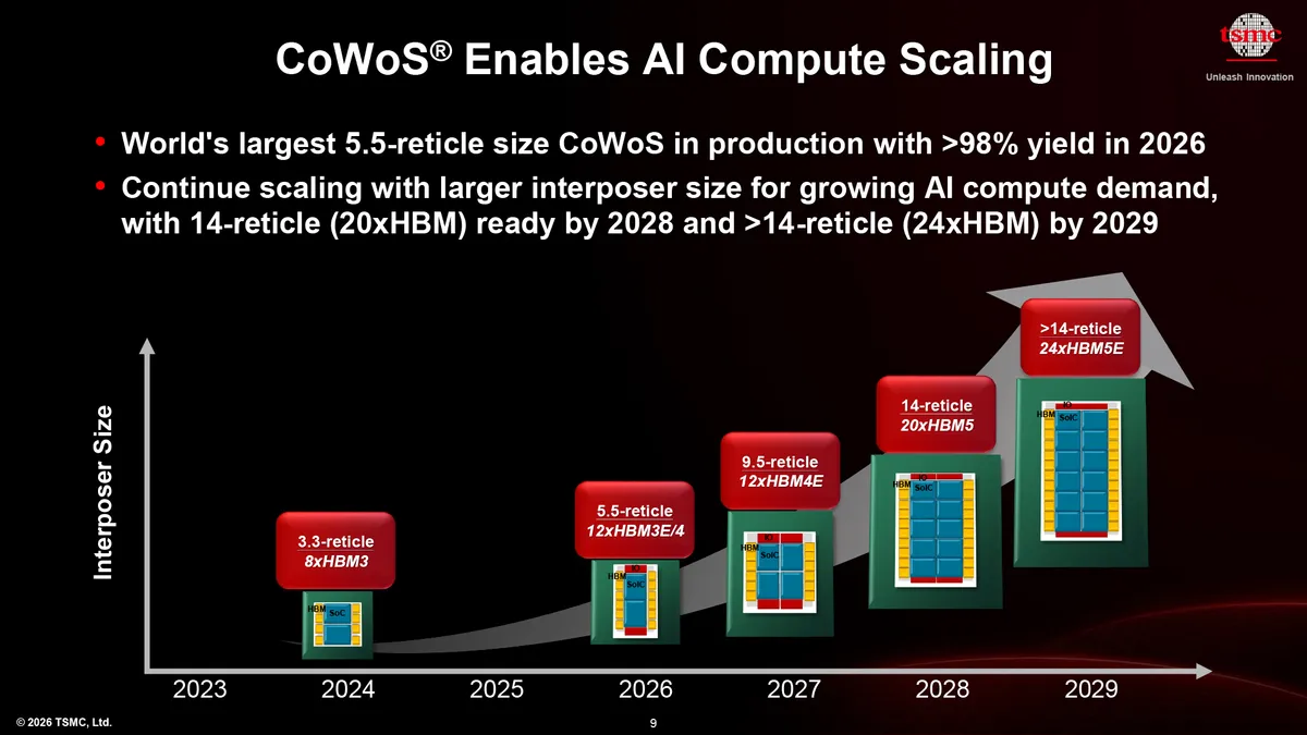
TSMC

(Image credit: TSMC)

But panel-level packaging cannot leverage the tools currently used for wafer-level packaging, as essentially technologies like CoWoS use the same lithography, etching, deposition, and other tools that were previously used to make logic chips. By contrast, panel-level integration tools are considerably less advanced.

 "From technology point of view, wafer-level-based process is far more advanced than panel," Zhang said. "I am not talking about just TSMC, I am talking about the industry as a whole. Wafer-level processing is where the most advanced manufacturing technology exists today. To move to panel-based manufacturing, the industry needs to improve panel processes rapidly so they can eventually offer a better next-generation solution relative to wafer-level technology."

Get Tom's Hardware's best news and in-depth reviews, straight to your inbox.

In fact, the main advantage that panels have over wafers is indeed larger package size: currently, TSMC can use 120mm×150mm substrates, next-generation CoWoS technologies will enable 150mm×250mm substrates, but even substrates the size of a hardcover book look pale compared to the initial 310mm×310mm panels. Furthermore, future packages can get to 515mm×510mm or even 750mm×620mm, which is larger than a wafer. When asked specifically whether CoPoS will complement CoWoS rather than replace it, Zhang essentially answered positively.

TSMC

(Image credit: TSMC)

 "I think that may be a way to look at it because it depends on the specific product configuration," Zhang said. "At some of the product will continue to get optimum benefit by leveraging wafer-level processing capability. Our goal is to offer our customer all the options they would need in order to find the optimum solution for their next-generation product. CoWoS today [has a lot of] scaling room for us to continue to drive this technology forward. But at the same time, we are looking at a fan-out-based process, some use the word CoPoS, as another alternative path going forward."

TSMC is currently expected to complete its first CoPoS pilot line this June. The gap between pilot and meaningful production is often around two or three years, so a reasonable expectation for high-volume manufacturing (HVM) using CoPoS would be 2028 – 2029. However, keeping in mind that CoPoS uses new tools and since the peculiarities of these tools are unknown, it is more reasonable to expect the first CoPoS-based products in 2029 or 2030, with more meaningful volumes sometime in the first half of the next decade. At the end of the day, CoWoS existed for years before explosive adoption, so CoPoS will likely repeat this pattern.

Google Preferred Source

Follow Tom's Hardware on Google News, or add us as a preferred source, to get our latest news, analysis, & reviews in your feeds.

Anton Shilov is a contributing writer at Tom’s Hardware. Over the past couple of decades, he has covered everything from CPUs and GPUs to supercomputers and from modern process technologies and latest fab tools to high-tech industry trends.