







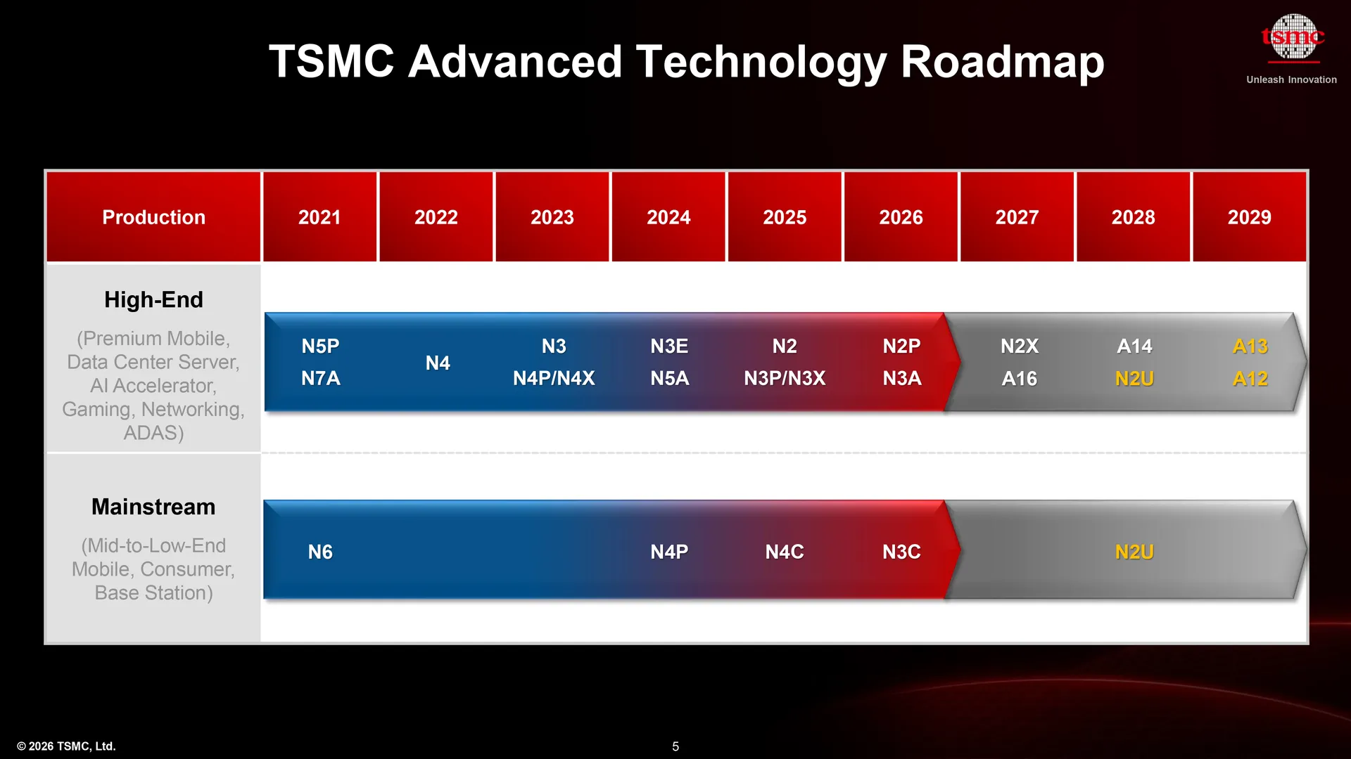
TSMC revealed its general manufacturing technology roadmap through 2029 at its North American Technology Symposium 2026 on Wednesday. Among the key highlights the company presented were its 1.2nm and 1.3nm-class fabrication processes called A12 and A13, an unexpected extension of the N2 family named N2U, and the lack of plans to use High-NA EUV lithography for any nodes through 2029. Perhaps the most notable part of the technology-related announcement was firming the multi-faceted approach to new node development.
Go deeper with TH Premium: Chipmaking
"Last year we announced A14 as our most advanced, 2nd Generation nanosheet technology, scheduled for production in 2028," said Kevin Zhang, senior vice president of business development and global sales and deputy COO at TSMC.
"This year, we are introducing derivatives of A14, including A13 and A12, both planned for production in 2029. A13 is an incremental enhancement of A14 achieved primarily through optical shrink, delivering about 6% area reduction while maintaining full design-rule and electrical compatibility, enabling customers to benefit with minimal redesign."
Changing the rules of the game
Historically the lion's share of TSMC's revenue originated from the smartphone industry, but more recently AI and HPC have outpaced handsets. This was clearly reflected in the company's plans, so TSMC's latest roadmap highlighted a deliberately bifurcated strategy that segments leading-edge nodes by end-market requirements rather than pursuing a one-size-fits-all approach. As a result, the company is adopting a new strategy for process technology introductions in which it will continue to offer a new node for client applications every year and will roll-out a new node for heavy-duty AI and HPC applications every two years.
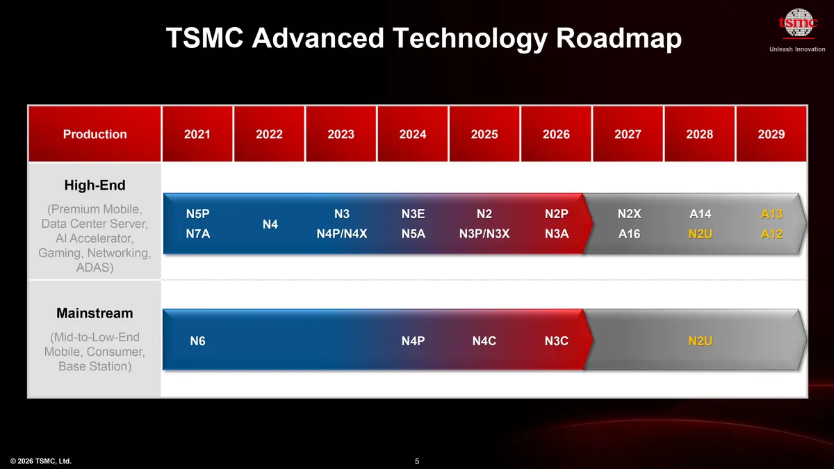
On one hand, processes like N2, N2P, N2U, A14, and A13 are aimed at smartphones and client devices — where costs, power efficiency, and IP reuse are crucial and strong design compatibility is welcome, while incremental improvements can be tolerated as long as TSMC can deliver a new node every year.
On the other hand, nodes such as A16 and A12, aimed at AI and HPC application, must offer strong performance improvements to justify transition to newer technologies, and costs are less important. These nodes integrate Super Power Rail backside power delivery (SPR) to address power integrity and current delivery constraints of AI data center and HPC workloads and offer tangible performance, power, and transistor density improvements — albeit, at a biennial cadence.
Swipe to scroll horizontally
| Row 0 - Cell 0 | A16 vs N2P | N2X vs N2P | N2U vs N2P | A14 vs N2 | A13 vs A14 | A12 vs A16 |
Power | -15% ~ -20% | lower | 8% - 10% | -25% ~ -30% | ? | lower |
Performance | 8% - 10% | 10% | 3% - 4% | 10% - 15% | ? | higher |
Chip Density* | 1.07x - 1.10x | ? | ? | 1.2x | ? | denser |
Logic Density | ? | ? | 1.02X - 1.03X | 1.23x | 1.06X | denser |
Transistor | GAA | GAA | GAA | 2nd Gen GAA | 2nd Gen GAA | 2nd Gen GAA |
Power Delivery | SPR | Front-side w/ SHPMIM (?) | Front-side w/ SHPMIM (?) | Front-side w/ SHPMIM (?) | Front-side w/ SHPMIM (?) | SPR |
HVM | 2027 | 2027 | 2027 | 2028 | 2029 | 2029 |
*Chip density published by TSMC reflects 'mixed' chip density consisting of 50% logic, 30% SRAM, and 20% analog.
**At the same area.
***At the same speed.
A13 and N2U: New nodes for client applications
Last year TSMC introduced its A14 process technology, which is set to rely on the company's 2nd Generation gate-all-around (GAA) nanosheet transistors, offer additional design flexibility with NanoFlex Pro technology, and serve as the foundry's premium node for high-end smartphone and client applications sometimes in 2028. This year the company announced A13, which will build upon A14.
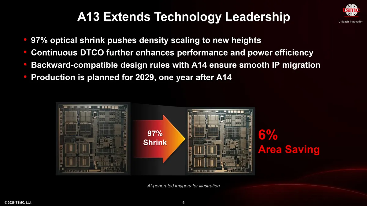
TSMC's A13 is an optical shrink of A14 designed to extract additional efficiency with minimal disruption. A13 reduces linear dimensions by about 3% (to ~97% scale), which translates into roughly 6% higher transistor density amid maintaining full design-rule and electrical compatibility with A14. From many points of view, A14 continues TSMC's long-standing tradition of offering optical shrinks of its process technologies (N12, N6, N4, N3P) — though, previously, these could deliver more tangible benefits in general. The approach enables TSMC's customers to reuse IP with little to no redesign effort, but with only incremental improvements.
While A14 is set to deliver full-node improvements in power, performance, and density, to extract them, chip and IP designers must use all-new tools, IPs, and design methodologies. By contrast, A13 delivers incremental gains enabled by design-technology co-optimization (DTCO), but which does not require to change anything to extract these gains. A13 is expected to enter production in 2029.
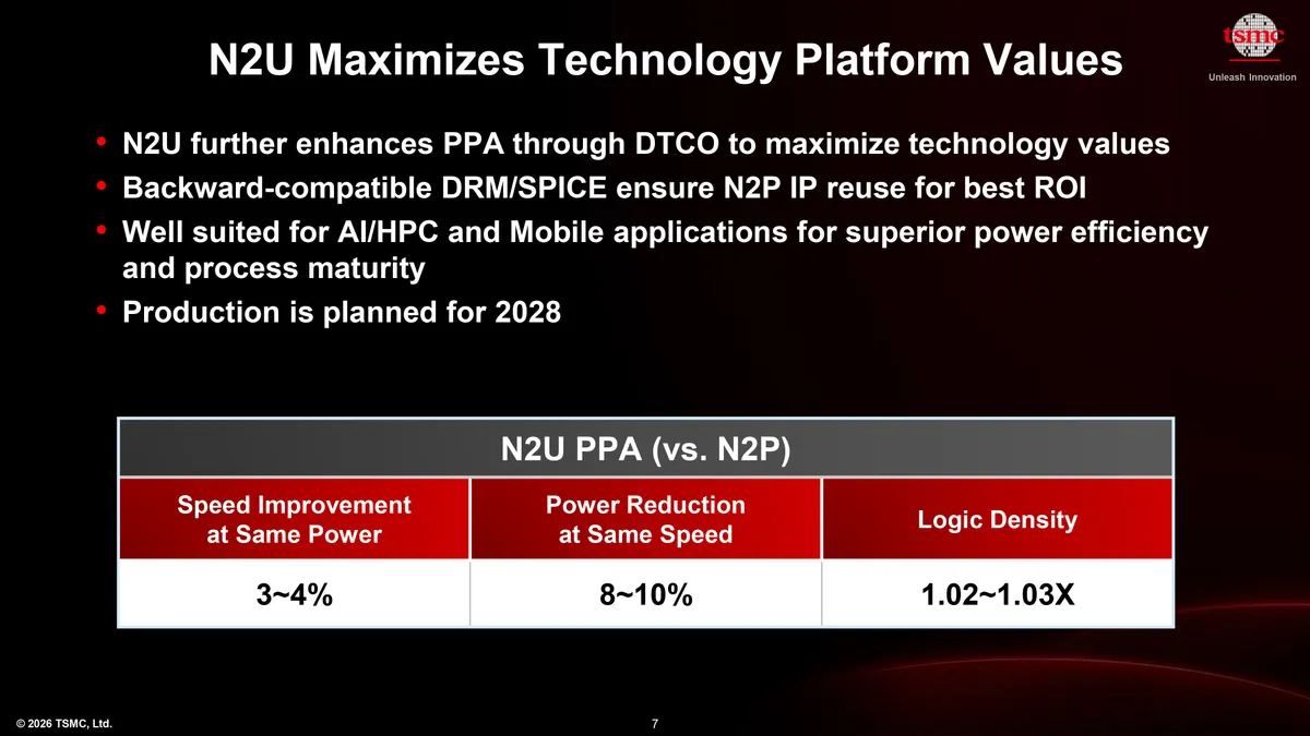
In addition to offering customers its all-new A14 node in 2028, TSMC plans to offer them a cheap way to improve their N2-based designs with N2U. N2U will be the third-year extension of the N2 platform that leverages DTCO to provide about 3% – 4% higher performance at the same power or 8% – 10% lower power at the same speed while allowing a modest 2% – 3% logic density improvement. The node will maintain compatibility with N2P IP, which will enable its customers (particularly from the client space) to build new products without transition to an all-new process and incur rather massive costs. For example, if a company plans to build a mid-range product using IP of a high-end product implemented using N2P in 2027, it can do it with N2U in 2028.
"We continue to extend our 2nm platform with N2U, which provides additional improvements in performance, power, and density through design-technology co-optimization," Zhang said. "Our strategy is to continue enhancing each node after introduction, allowing customers to maximize the return on their design investments while still gaining incremental PPA benefits."
A16, A12, and N2X: Maximum performance at any cost
While TSMC's N2 is set to be adopted both for client and data center applications, the company preps A16 with its Super Power Rail backside power delivery that is specifically tailored for high performance data center applications. Essentially, A16 is N2P with SPR that will rely on the 1st Generation nanosheet GAA transistors and provide significant power, performance, and transistor density advantages over N2 and N2P nodes, albeit at higher cost.
It is noteworthy that TSMC now lists A16 as a 2027 process technology, which is technically a slip from 2026.
"A16 will be ready for production in 2026," Zhang said. "However, actual product ramp depends on customers, and we expect volume production to begin in 2027. That is why we aligned it to that timeline."
Interestingly, the arrival of A16 does not replace N2X, a performance-enhanced variant of N2P that uses traditional front side power delivery to push clocks of N2-based designs to the max.
A16 will pass the baton to A12 — set to arrive in 2029 — which is projected to bring full-node advantages to TSMC's data center-class nodes. While TSMC does not disclose actual numbers, expect A12 to offer the same kinds of benefits over A16 as A14 brings over N2 as it is set to rely on the company's 2nd Gen nanosheet GAA transistors and NanoFlex Pro technology.
“I can say that A16 is our first-generation technology with Super Power Rail, or backside power delivery, and A12 is the next generation,” Zhang said. “A13 and A12 are built on A14 with significant geometric scaling. To continue shrinking the frontside geometry, you also need to scale the backside to achieve overall density benefits. So there are many enhancements being implemented as we move from A16 to A12, particularly related to backside power delivery. That is all I can share.”
No High-NA on horizon
One interesting thing to note about TSMC's upcoming A13 and A12 process technologies due in 2029 is that none of them will require High-NA EUV lithography tools, which is stark contrast to Intel's approach to its 14A production node and successors that are set to use High-NA EUV scanners starting in 2027 – 2028.
"I tell you, I am amazed by our R&D team," said Kevin Zhang. "They continue to find a way to drive the technology scaling without using High-NA. One day they may have to use it, but at this point, we continue to be able to harvest the benefit from current EUV, not have to go to High-NA, which, you know, very, very expensive."

Follow Tom's Hardware on Google News, or add us as a preferred source, to get our latest news, analysis, & reviews in your feeds.