


惯性聚合 高效追踪和阅读你感兴趣的博客、新闻、科技资讯
阅读原文 在惯性聚合中打开

推荐订阅源

Stack Overflow Blog
Stack Overflow Blog
J
Java Code Geeks
Last Week in AI
Last Week in AI
人人都是产品经理
人人都是产品经理
博客园 - 【当耐特】
钛媒体:引领未来商业与生活新知
钛媒体:引领未来商业与生活新知
C
Check Point Blog
月光博客
月光博客
腾讯CDC
Engineering at Meta
Engineering at Meta
博客园 - Franky
Vercel News
Vercel News
D
Docker
OSCHINA 社区最新新闻
OSCHINA 社区最新新闻
F
Fortinet All Blogs
Microsoft Security Blog
奇客Solidot–传递最新科技情报
奇客Solidot–传递最新科技情报
雷峰网
雷峰网
Google DeepMind News
Martin Fowler
Martin Fowler
GbyAI
GbyAI
B
Blog
Hugging Face - Blog
Hugging Face - Blog
T
Tailwind CSS Blog

Latest from Tom's Hardware in News

Analytics group signals possible delays at 40% of AI data center construction sites — companies deny schedule holdups, but satellite imagery indicates otherwise Intel hires tenured Samsung exec to lead Foundry Services — signals company focus on winning business from potential Foundry suitors Elon Musk pushing forward with Terafab at Microsoft's April patch puts Windows domain controllers into reboot loops — third known issue from KB5082063… AMD Ryzen 9 9950X3D2 appears on Amazon with $1,000 pre-order price — AMD confirms recommended pricing is still set… AMD's market cap hits all-time high, Intel hits 25-year high on Agentic AI's insatiable demand for CPUs Meta raising Quest headset prices due to AI-driven RAM shortage — Quest 3 to cost $600, Quest 3S $350 from April… Elegoo announces the Jupiter 2 resin 3D printer for $949, early bird price of $849 — new model offers massive print volume but is still physically smaller than previous models Pragmata PC performance tested: 18 GPUs take us to the Moon Chinese fabs import record volumes of US chipmaking equipment via Singapore and Malaysia — homegrown tool makers booked record 2025 revenues as price competition squeezes margins US appeals court restarts $3 billion patent infringement lawsuit against Intel — VLSI case from 2017 returns after… Two US citizens get combined 16 years in prison for running North Korean laptop farms — fake remote IT work scheme netted DPRK $5 million in around three years Intel launches Wildcat Lake as Core Series 3 for value laptops and edge systems — six consumer SKUs built on 18A promise Legendary Qualcomm, Apple, and Nuvia alumni form new CPU startup — Nuvacore promises to Bambu updates its 3D printers to print unique hues or gradients using two or three filaments — company acknowledges OrcaSlicer-FullSpectrum fork as the basis for the color prediction part of the new feature Broadcom to supply Meta with custom silicon through 2029 — Broadom CEO Hock Tan departs Meta Anonymous perps behind 86 million files scraped from Spotify hit with $322 million court judgement — Anna Non-functioning counterfeit Samsung 990 Pro SSDs are circulating in Europe — Despite convincing packaging, blue… Oklahoma farmer arrested and jailed for trespassing during AI data center town hall — removed by officers after going a few seconds over allotted speaking time, trying to hand paperwork to counselors Virginia voter support for new data centers collapses from 69% in 2023 to 35% in new poll — Multi-gigawatt, 37-building Digital Gateway project abandoned Struggling shoemaker and apparel brand Albird pivots to AI data centers, stock jumps 580% in a single day — sells core business and leveraging $50 million in financing to become a GPU-as-a-Service and AI cloud solutions provider IPv6 usage reaches historic 50% across Google services, matching IPv4 — increased usage eases pressure on the IPv4 address market as 'new' protocol designed in 1998 finally hits its stride Engineer open-sources DIY radar system that's 95% cheaper than $250,000 commercial offerings, has 20 kilometer range — Moroccan engineer designs Aeris-10 radar, shares it on GitHub Elon Musk demonstrates first sample of Tesla AI5 processor, accidentally thanks TSC rather than TSMC  — claims 40X performance boost over the predecessor Valve might be adding a 30-day price tracker to Steam — feature is already available in some EU countries to spoof… Memory cards and flash drives prices rocket 124%, some products peak at 261% jump — increases from 2025 driven by AI chip shortage across a range of formats and capacities Netgear secures conditional approval from the FCC following router ban — company can continue importing foreign-made routers through October 2027 China tests deep-sea electro-hydrostatic actuator that can cut undersea cables at a depth of 3,500 meters — state hails successful trial and hints at deployment readiness Iran reportedly bought an in-orbit Chinese satellite to target US military sites in the Middle East — purchase agreement included ongoing ground control services based in China Our lifestyle tech colleagues at Tom's Guide have overhauled their site for smarter shopping — more video and access to experts make it 'the biggest relaunch in our history'
Chinese startup claims photonic chip production without D...
Etiido Uko · 2026-06-09 · via Latest from Tom's Hardware in News
Prinano
(Image credit: Prinano)

Chinese semiconductor start-up Prinano announced that it has successfully validated the mass production of photonic chips without using the industry-standard lithography equipment. According to an SCMP report, the company said in a WeChat post on Friday, June 5th, that it had made 8-inch optical chip wafers in collaboration with Shenzhen Litra Technology. The company said it achieved this while “completely avoiding” the need for deep-ultraviolet lithography (DUV), a significant breakthrough in China’s push to reduce its dependence on ASML lithography tools, which remain subject to export restrictions.

Go deeper with TH Premium: Chipmaking

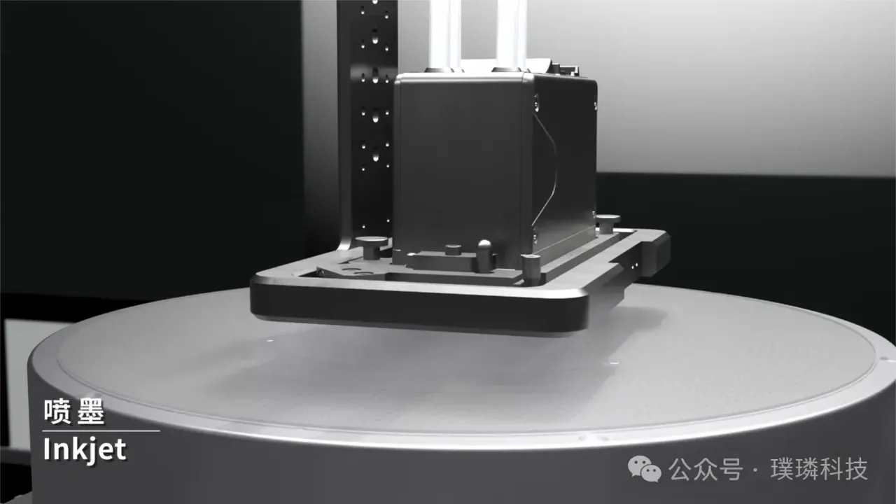
Instead of conventional optical lithography, Prinano said it used its PL-AS vacuum air-cushion nanoimprint lithography (NIL) system, which, according to the company, can reduce manufacturing costs to roughly one-tenth that of traditional DUV-based processes, while supporting wafer-level production of photonic chips.

Modern chips are typically produced using highly sophisticated DUV or more advanced EUV (extreme ultraviolet) systems that project circuit patterns onto silicon wafers using light. These machines contain some of the most complex optics ever built and can cost hundreds of millions of dollars. Nanoimprint lithography takes a very different approach. Rather than projecting patterns using light, it physically presses nanoscale structures into a specially prepared resist layer, basically stamping microscopic patterns directly onto the wafer surface. This process eliminates the need for many of the expensive optical systems required by conventional lithography equipment.

Nanoimprint lithography has long been viewed as a potential alternative to conventional optical lithography because of its potential for lower costs and extremely high pattern resolution. However, despite its promise, the technology has struggled to achieve widespread adoption in semiconductor manufacturing due to concerns about defect rates, template wear, throughput, and production yields, all of which become increasingly important in high-volume manufacturing environments.

Founded in 2017, Prinano has spent the past several years working to overcome those limitations by developing its own nanoimprint lithography ecosystem. The company took a significant step in 2025 when it announced the delivery of what it described as China's first semiconductor nanoimprint lithography system to a domestic customer, marking an early effort to commercialize the technology.

The company's latest announcement suggests it may have progressed beyond equipment development and pilot deployments. According to Prinano, its PL-AS vacuum air-cushion nanoimprint lithography platform incorporates wafer-level pressure control, customized double-layer imprinting materials, and proprietary process technologies capable of producing sub-10-nanometer features. The company now claims those developments have enabled the successful validation of wafer-scale photonic chip production on 8-inch wafers.

Importantly, Prinano is not attempting to replace the production of cutting-edge processors or AI accelerators. Instead, the company's announcement focuses on photonic chips, a category of semiconductors that manipulate light rather than electrical signals. These devices are widely used in fiber-optic communications, data center interconnects, sensing systems, and LiDAR technologies.

Get Tom's Hardware's best news and in-depth reviews, straight to your inbox.

Photonic chips are considered particularly well suited to nanoimprint lithography because many of their critical structures, including waveguides, gratings, and ring resonators, consist of repeating nanoscale patterns that can be replicated efficiently through imprinting techniques. This characteristic makes them a more practical near-term application for NIL than advanced logic chips, where defect rates and alignment requirements are far more demanding.

Another noteworthy detail is the use of 8-inch wafers. While leading-edge processors are increasingly manufactured on larger 12-inch wafers, 8-inch wafers remain widely used across specialized sectors such as compound semiconductors and power electronics. Demonstrating production on full 8-inch wafers suggests the process has moved beyond laboratory-scale demonstrations and into a format more compatible with commercial manufacturing.

The development also highlights China's broader search for alternative semiconductor manufacturing pathways amid ongoing export restrictions. Access to advanced lithography equipment from ASML — required for EUV and DUV — has been increasingly constrained under US-led controls, prompting Chinese companies to explore alternative approaches ranging from advanced packaging technologies to new chip architectures and novel manufacturing methods. Huawei recently announced a new LogicFolding chip architecture that allows the company to develop high-performance processors without relying on restricted EUV lithography machines.

Significant questions remain about Prinano’s announcement. While the claims have been validated in mass production, the company did not disclose production volumes, yield rates, defect densities, customer shipment data, or independent third-party validation. These metrics are critical for determining whether a semiconductor manufacturing technology is commercially viable rather than merely technically feasible.

Google Preferred Source

Follow Tom's Hardware on Google News, or add us as a preferred source, to get our latest news, analysis, & reviews in your feeds.

Etiido Uko is a news contributor for Tom's Hardware covering the latest updates in big tech and the PC industry. He is a mechanical engineer and senior technical writer with over nine years of experience in documentation and reporting. He is deeply passionate about all things engineering and technology, and is an expert in gadgets, manufacturing, robotics, automotive, and aerospace.