
惯性聚合 高效追踪和阅读你感兴趣的博客、新闻、科技资讯
阅读原文 在惯性聚合中打开

推荐订阅源

H
Help Net Security
腾讯CDC
爱范儿
爱范儿
Google DeepMind News
V
V2EX
Blog — PlanetScale
Blog — PlanetScale
Engineering at Meta
Engineering at Meta
GbyAI
GbyAI
量子位
F
Fortinet All Blogs
G
Google Developers Blog
T
The Blog of Author Tim Ferriss
Cyber Security Advisories - MS-ISAC
Hugging Face - Blog
Hugging Face - Blog
Last Week in AI
Last Week in AI
T
Tailwind CSS Blog
J
Java Code Geeks
S
SegmentFault 最新的问题
D
Docker
博客园 - 司徒正美
The GitHub Blog
The GitHub Blog
Jina AI
Jina AI
M
MIT News - Artificial intelligence
博客园 - 【当耐特】

Latest from Tom's Hardware in Semiconductors

Intel Intel’s performance-enhanced 18A-P process enters risk production — drop-in 18A upgrade promises 9% performance improvement at iso-power, cuts thermal resistance by 40% Chinese fab SMIC TSMC says panel packaging won Analyzing TSMC's fab expansion roadmap — multi-fab N2 ramp, CoWoS, SoIC, and uncorking bottlenecks Chinese startup claims photonic chip production without DUV lithography, says nanoimprint process cuts costs by 90%… ASML becomes Europe's most valuable company ever as analysts bet on higher EUV output — its market cap hit… TSMC CEO C.C. Wei says, ‘It will be a long time before we can meet customer demand’ — tells shareholders that he will keep prices stable, refrain from implementing price hikes Samsung shows first HBM5 mockup with Heat Path Block cooling — thermal race with SK hynix shaping up Seven hospitalized after toxic gas fire at SK hynix advanced memory plant — Cheongju 4th campus incident today led… TikTok owner ByteDance is reportedly developing its own custom AI CPUs — company looks to ease China's… Trailing-edge foundry roadmaps for GlobalFoundries, UMC, and SMIC — mature node chipmakers each pursue differing… Chinese university builds 3D chip design tool tailored to Huawei's ‘LogicFolding’ architecture — 3D design delivers increased performance and better thermal management China adds homegrown AI chips to 'secure and reliable' procurement list for the first time — nine options added as move away from Nvidia continues SK hynix unveils 'iHBM' thermal architecture that cools AI memory at the source — integrated cooling elements inside HBM interface cut thermal resistance by 30%, target next-gen HBM5 accelerators and dense AI data centers Imec builds world's first High-NA EUV-fabricated quantum dot qubit device — breakthrough could pull quantum computing onto the same manufacturing roadmap as next-gen AI processors, compressing timelines Huawei claims sanctions-busting breakthrough with 1.4nm-class chips by 2031, claims 55% higher transistor density — firm claims new LogicFolding chip architecture can bypass EUV restrictions, introduces 'Tau Scaling Law' to replace Moore's Law Samsung's $400,000 payout for memory workers sparks revolt as other divisions get only $4,000, fueling intentional production slowdowns — internal resentment disrupts packaging operations, major AI chip project decisions to a complete halt The custom AI ASIC state of play (May 2026) — Broadcom deals, Google TPUs, Meta MTIA & beyond AMD begins production ramp of 256-core EPYC Venice — first 2nm HPC chip claims 70% performance leap Intel kicks off development on next-decade 10A and 7A process technologies — 14A node remains on track for… SMIC founder and AMEC CEO urge Chinese fabs to test domestic chipmaking tools on active production lines — equipment makers post record revenue but falling margins Russia’s Mikron is selling framed test wafers with up to 120,000 processors as souvenirs — 12 designs, priced around $170 each, sold alongside $2 vials of cleanroom air Trump calls $14 billion Taiwan arms deal a 'negotiating chip' with China after Xi said Taiwan issue could lead to 'clashes and even conflicts' — Trump says 'Taiwan would be very smart to cool it a little bit' Leading-edge foundry roadmaps for TSMC, Intel and Samsung — outlining the path to 1.4nm nodes and beyond TSMC allocates $20 billion to Arizona expansion — project faces water and labor shortages, complicated by visa… NASA partners with Microchip to build next-generation spaceflight chips with 100x the power of current offerings — chip designed to withstand radiation for extended missions on the Moon and Mars Intel, SK hynix shares surge following reports of chip packaging partnership — SK is said to be testing… Apple reportedly strikes deal for Intel to make some of its chips — two tech giants reached a preliminary… Global semiconductor sales hit nearly $300 billion in Q1 2026 — chips are on track to top $1 trillion for this…
Post-silicon era gets closer as industry giants crack the...
https://www.tomshardware.com/author/luke-james · 2026-06-19 · via Latest from Tom's Hardware in Semiconductors
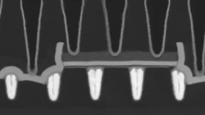
300mm integration of 2D-material transistors
(Image credit: imec/ASML/TSMC)

Imec, ASML, and TSMC have integrated both n-type and p-type transistors with atomically thin 2D channels on a single 300mm wafer at a 50nm contacted poly pitch, the tightest pitch demonstrated to date for complementary 2D devices and one that lands within range of leading-edge silicon.

The trio presented the work this week at the IEEE/JSAP Symposium on VLSI Technology and Circuits, using a single EUV exposure to print channel lengths as short as 28nm. Imec reported that 94% of the integrated transistors switched correctly, with an on/off current ratio above 100,000. The n-channel devices use molybdenum disulfide (MoS2), while the p-channel devices use tungsten diselenide (WSe2) or tungsten disulfide (WS2).

Luke James is a freelance writer and journalist.  Although his background is in legal, he has a personal interest in all things tech, especially hardware and microelectronics, and anything regulatory.