


It's the world’s first sub-1 nm chip technology, IBM claims. The fingernail-size chip is built with IBM's new transistor architecture, called nanostack, which vertically stacks and staggers transistors to pack more onto a chip.
IBM is showing off a fingernail-size silicon chip that promises to deliver more power, more efficiently, in future computing, communications, and infrastructure deployments.
The sub-1 nanometer (nm) chip features a transistor architecture at the 0.7 nm, or 7 angstrom node, IBM says. It packs nearly 100 billion transistors, which is almost twice the density of IBM’s 2 nm chip unveiled in 2021.
A series of structural and material innovations made the chip possible, according to IBM, including its three-dimensional nanostack architecture. That’s a way of stacking different types of chips vertically, rather than spreading everything out side-by-side on a circuit board, according to Jay Gambetta, director of IBM Research and IBM Fellow. It allows those layers to communicate through extremely short vertical connections, he says.
“With our new nanostack architecture, we’re not just making smaller transistors, we’re reinventing how chips are built to deliver dramatically more power and energy efficiency,” Gambetta said. The technology demonstrates how continued gains in performance and efficiency remain possible even as chip features approach atomic dimensions and the industry faces the physical limits of traditional chip scaling, he said.
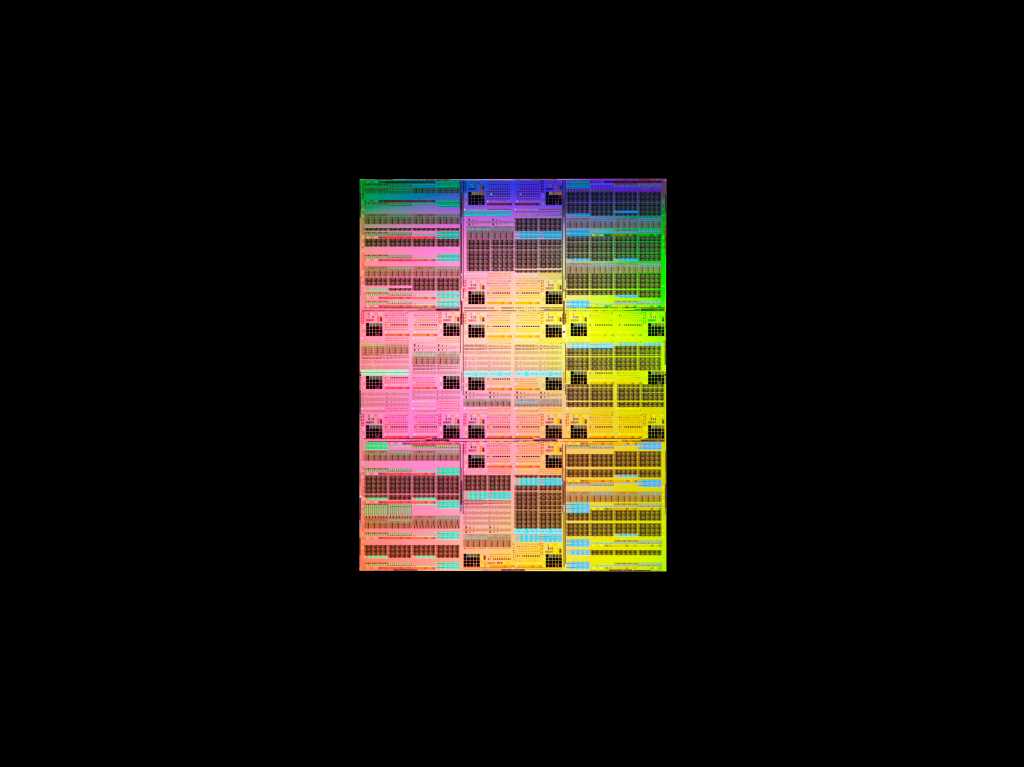
It’s the world’s first sub-1 nm chip technology, IBM claims.
IBM
The new chip is projected to offer up to 50% more performance, or 70% greater energy efficiency than IBM’s 2 nm node chips.
“With these sorts of power gains, the potential for 7 angstrom devices is sky high, with a massive potential impact on the world of AI. Today’s popular AI accelerators can produce about 1,500 TOPS (or trillions of operations per second), and IBM researchers estimate one using 7 angstrom technology could deliver about six times more, or around 9,000 TOPS. So if 7 angstrom chips were used to train today’s massive, frontier-model LLMs, we could drastically cut a typical training time from around three months to a couple weeks,” Mike Murphy of IBM research wrote in a blog about the new chip.
In addition, IBM researchers demonstrated that the nanostack architecture provides 40% scaling in Static Random-Access Memory (SRAM), giving chip designers much more efficient chips while also supporting the high-bandwidth data demands of advanced AI workloads, Gambetta said.
Unlike standard Dynamic RAM (DRAM), SRAM holds data without needing to be constantly refreshed, making it faster and more reliable for high-performance, high-frequency applications and workloads.
“The team has managed to scale up SRAM (or static random-access memory) by 40% in the 7 angstrom design. It’s a massive leap in memory capacity — the likes of which the industry hasn’t seen in over a decade,” Murphy wrote. “Accessing on-chip memory is one of the key bottlenecks in AI computing that the team has addressed with the new 7 angstrom design, ensuring these chips will be able to process information much more rapidly than previous designs could. And by shrinking the physical footprint of memory, you can pack more capacity into the same amount of space.”
Using the nanostack architecture, IBM’s semiconductor roadmap projects at least a decade of future scaling, according to Gambetta. As for when this technology could be used in real products, IBM said it is targeting production in the next five years.
IBM has over the years invented much of the underlying technologies that drive intelligent silicon production. For example, Big Blue was one of the key developers of copper-wired chips in 1997 when aluminum was the standard. It was also instrumental in developing other chip technologies, such as silicon-based insulators, metal gate transistors, nano-gate transistors, and 2 nm chips.
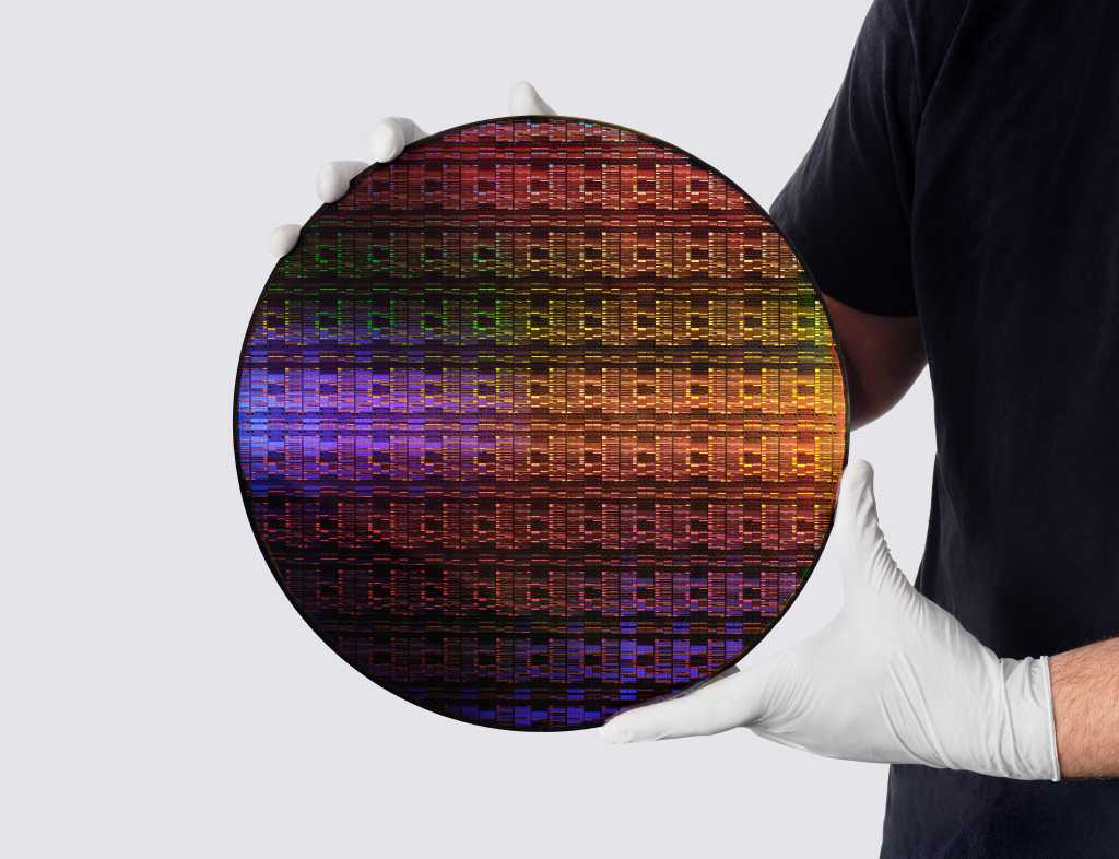
Researcher holds IBM’s sub-1 nm node wafer.
IBM
SUBSCRIBE TO OUR NEWSLETTER
From our editors straight to your inbox
Get started by entering your email address below.