


Each GPU generation pushes against the same constraint: memory. Models grow faster than memory capacity, forcing engineers into complex multi-GPU setups, aggressive quantization, or painful trade-offs.
NVIDIA's Blackwell architecture, succeeding Hopper in 2024, attacks this problem at the hardware level, rethinking not just how much memory a GPU has, but how it's structured and accessed entirely.
Running Llama 3 70B is no longer a concern – no parallelization or squeezing the model into tight memory limits. Instead, the same hardware footprint can now handle significantly larger parameter counts.
This article breaks down the memory enhancements that make Blackwell the most capable AI accelerator to date.
Prerequisites
This article assumes you're comfortable with a few GPU fundamentals. If any of these feel shaky, the linked resources will get you up to speed in 10–15 minutes each.
GPU anatomy — what an SM is, and the role of registers, shared memory (L1), L2 cache, and memory controllers. [Memory Hierarchy of GPUs]
The three memory metrics — capacity (how much fits), bandwidth (how fast data moves), and latency (how long a single access takes). These aren't interchangeable, and Blackwell improves all three differently. [GPU Memory Bandwidth]
GPU memory types — HBM, GDDR, and LPDDR5X, and the bandwidth/capacity/power trade-offs between them. [Cuda GPU Memory Types]
Chip interconnects — PCIe, NVLink, and the idea of a chip-to-chip (C2C) link. [The AI Systems Game]
If you're solid on all four, you're ready.
Table of Contents
The Generational Leap
Before diving into how Blackwell achieves its performance gains, here's what changed from the previous GPU generation:
| Spec | Hopper H100 | Blackwell B200 | Change |
|---|---|---|---|
| HBM Capacity | 80 GB (HBM3) | 192 GB (HBM3e) | 2.4× |
| HBM Bandwidth | 3.35 TB/s | 8 TB/s | 2.4× |
| L2 Cache | 50 MB | 126 MB | 2.5× |
| L1/Shared per SM | 256 KB | 128 KB | 0.5× |
| Die Design | Monolithic | Dual-die (MCM) | — |
| CPU Integration | Separate (PCIe) | Unified (NVLink C2C) | — |
The numbers tell a clear story: more memory, more bandwidth, larger caches. The rest of this article explains how these pieces fit together
The GB200 Superchip
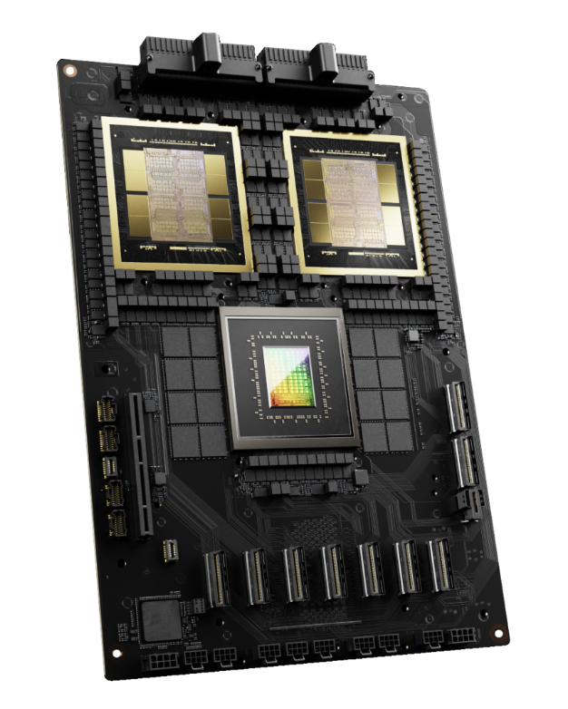
The Grace Blackwell (GB200) extends the superchip design NVIDIA introduced with the Grace Hopper (GH200), where an ARM-based Grace CPU is paired with GPU chips in a single package to form one unified computing system.
In the Blackwell generation, the GB200 pairs one Grace CPU with two Blackwell GPUs, connected via NVLink Chip-to-Chip (NVLink-C2C), a high-bandwidth interface that lets the CPU and GPUs share memory and operate as a single system.
Grace CPU
The Grace CPU is an ARM Neoverse v2 designed by NVIDIA for bandwidth and efficiency. It handles general-purpose tasks, pre-processing, and tokenization, and feeds data to the GPU through NVLink C-2-C. The Grace CPU acts as extended storage for the GPU.
The Grace CPU runs at a moderate clock speed but compensates with a large memory bandwidth of up to 500GB/s to its LPDDR5X memory (Low Power Double Data Rate 5x – we'll discuss this more in a moment) with about 100MB of L3 Cache.
LPDDR5X (Low Power Double Data Rate 5x)
The LPDDR5X is a high-speed memory standard that delivers data up to 10.7 Gbps. The LPDDR5X offers low-power efficiency, making it ideal for this use case.
It strikes a perfect balance between performance and power efficiency, delivering up to 500 GB/s while using only about 16W, roughly one-fifth the power of conventional DDR5 memory.
Blackwell GPU
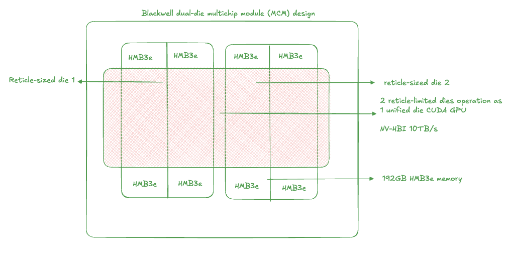
The Blackwell GPU made significant improvements over the previous Hopper GPU model, especially in terms of memory. The Blackwell GPUs are designed as dual-die GPUs, with two GPU dies in a single module.
Each die is connected by a super-fast NV-HBI (NVIDIA High-Bandwidth Interface) with a speed of 10TB/s, ensuring full performance. Each die contains 104 billion transistors, totaling 208 billion across the two dies. Each die also contains 96 GB of HBM3e memory, totaling 192 GB, with 180 GB usable (as 12 GB is used for error-correcting code (ECC), system firmware, and so on).
With this amount of memory, the Blackwell GPU's memory bandwidth is about 2.4 times faster than that of the Hopper generation.
The L2 cache was also increased to 126 MB. By increasing the L2 cache, Blackwell can store more neural network weights or intermediate results on-chip, avoiding extra trips out to HBM. This ensures the GPU’s compute units are rarely starved for data.
High-Bandwidth Interface (NV-HBI)
High Bandwidth Interconnect is a standard for die-to-die (or d2d) communication. The NVIDIA High-Bandwidth Interface (NV-HBI) offers a 10TB/s connection, combining the two GPU dies into a single, unified GPU.
NVLINK C-2-C (Chip-to-Chip)
The NVLink C-2-C provides a communication speed of up to ~900 GB/s between the Grace CPU and the Blackwell GPUs, eliminating the need to copy memory from the CPU to the GPU memory pool via the PCIe bus.
The NVLink C-2-C interconnect speed is faster than the typical PCIe bus. PCIe Gen6 is only about 128 GB/s per direction compared to the NVLink C-2-C's speed. It's also cache-coherent, meaning both the CPU and GPU share a coherent memory architecture, allowing the CPU to read and write to GPU memory and vice versa.
This unified memory architecture is called Unified CPU-GPU Memory or Extended GPU Memory (EGM) by NVIDIA.
Memory Hierarchy and Bandwidth
Understanding how data flows through Blackwell's memory system is key to optimizing AI workloads. The architecture follows a classic hierarchy principle: smaller, faster memory sits closest to the compute units, with progressively larger but slower memory tiers extending outward.
The Hierarchy at a Glance
| Memory Tier | Capacity | Bandwidth | Purpose |
|---|---|---|---|
| Registers | ~256 KB per SM | Immediate | Active computation |
| L1/Shared Memory | ~128 KB per SM | ~40 TB/s aggregate | Data staging, inter-thread sharing |
| L2 Cache | 64-65 MB per die (~126 MB total) | ~20 TB/s | Cross-SM data reuse |
| HBM3e | 192 GB (180 usable) | 8 TB/s | Model weights, activations |
| LPDDR5X (CPU) | ~480 GB | ~500 GB/s (900 GB/s via NVLink C2C) | Overflow, large embeddings |
Registers and L1/Shared Memory
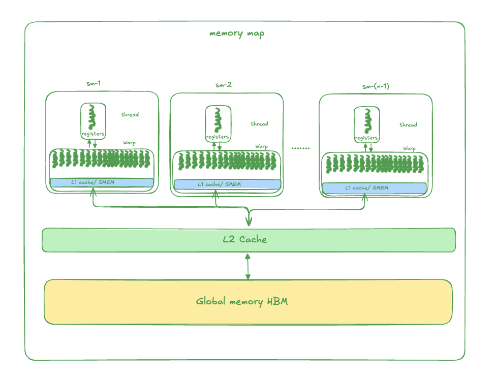
A streaming multiprocessor (SM) executes compute instructions on the GPU. At the lowest level, each Streaming Multiprocessor (SM) contains a register file and configurable L1/Shared memory as illustrated in the diagram above. Registers hold the operands for active computations, that is, data that the GPU cores are working on right now.
An SM executes threads in fixed-size groups known as warps, with each warp containing exactly 32 threads that execute the same instructions in lockstep. The L1/Shared memory acts as a staging area, allowing threads within an SM to share data without going to slower memory tiers.
Blackwell's L1/Shared memory is 128 KB per SM by default, a reduction from Hopper's 256 KB. In specific configurations, this can extend to 228 KB per SM. The aggregate bandwidth across all SMs is approximately 40 TB/s.
Why the reduction? NVIDIA shifted capacity to TMEM for Tensor Core operations and compensated with a larger L2 cache. General-purpose shared memory workloads see less per-SM capacity, but the workloads that matter most, matrix multiplications, get dedicated, faster memory.
L2 Cache: Compensating for Smaller L1
The L2 cache sits between the SMs and HBM, shared across all compute units on a die. Blackwell provides 64-65 MB per die (roughly 126 MB total across the dual-die module). This represents a 2.5× increase over Hopper's 50 MB and compensates for the smaller per-SM L1.
In AI workloads, the same model weights are accessed repeatedly across different input batches. A larger L2 cache means more of these weights can stay on-chip between batches, reducing expensive trips to HBM. For inference serving, where the same model handles thousands of requests, this translates directly to lower latency and higher throughput.
The dual-die design does introduce complexity here. Each die has its own 63 MB L2 partition. Accessing data cached on the other die requires crossing the NV-HBI interconnect fast at 10 TB/s, but still slower than local L2 access. NVIDIA's software stack handles this transparently, but performance-conscious engineers should be aware that data placement across dies can affect cache efficiency.
HBM3e: The Main Memory Pool
High Bandwidth Memory (HBM3e) serves as the primary storage for model weights, activations, gradients, and input data. Blackwell's HBM3e delivers 8 TB/s of bandwidth per GPU, roughly 2.4× faster than Hopper's 3.35 TB/s HBM3.
The physical implementation uses an 8-Hi stack design: eight DRAM dies stacked vertically, each providing 3 GB, for 24 GB per stack. With eight stacks total (four per die), the B200 GPU provides 192 GB of on-package memory, though 180 GB is usable after accounting for ECC and system overhead.
This bandwidth increase is critical. Tensor Core operations can consume data at enormous rates. If HBM can't feed data fast enough, the compute units stall, leaving expensive silicon idle. Blackwell's 8 TB/s keeps the tensor cores fed even during the largest matrix multiplications.
LPDDR5X: The Extended Tier
Beyond the GPU's HBM sits the Grace CPU's LPDDR5X memory, approximately 480 GB accessible at up to 500 GB/s locally, or ~900 GB/s when accessed from the GPU via NVLink C-2-C.
Accessing LPDDR5X from the GPU has roughly 10× lower bandwidth and higher latency compared to HBM. But it remains far faster than NVMe SSDs or network storage.
LPDDR5X serves as a high-speed overflow tier. Data that doesn't fit in HBM, such as large embedding tables, KV caches for long-context inference, or checkpoint buffers, can reside in CPU memory without catastrophic performance penalties.
Data Flow in Practice
When a Blackwell GPU executes an AI workload, data flows through this hierarchy in stages:
Model loading: Weights move from storage → CPU memory → HBM (or stay in LPDDR5X if HBM is full)
Batch processing: Input data streams into HBM, then into L2 as SMs request it
Computation: Active data moves from L2 → L1/Shared → Registers as operations execute
Output: Results flow back down the hierarchy to HBM or CPU memory
Each tier serves as a buffer for the tier above it.
Practical Example: Running Llama 3 70B
Consider deploying Llama 3 70B for inference. In FP16 precision (Note with GB200, you can go as low as FP4), the model weights alone require approximately 140 GB of memory.
On a Hopper H100 (80 GB HBM3): The model doesn't fit. You must either quantize aggressively, use tensor parallelism across multiple GPUs, or offload layers to CPU memory over PCIe (slow at ~64 GB/s).
On a single GB200 Superchip (~360 GB usable HBM3e + ~480 GB LPDDR5X): The full 140 GB model fits easily within a single GPU's HBM, leaving the second GPU's HBM and all CPU memory available for KV cache, batching, or running multiple model instances. No model parallelism required. No aggressive quantization forced by memory limits. The GB200 Superchip provides roughly 10× the usable memory of a single H100, fundamentally changing what fits on one unit
This is the practical impact of Blackwell's memory architecture: models that previously required multi-GPU setups can now run on a single superchip, simplifying deployment and reducing inter-GPU communication overhead.
Conclusion
Memory has always been the limiting factor in AI hardware. Blackwell changes that equation.
By combining dual-die GPUs, HBM3e with 8 TB/s bandwidth, and unified CPU-GPU memory through NVLink C2C, NVIDIA has delivered a system where a single superchip offers roughly 10× the usable memory of its predecessor. Models that once demanded complex multi-GPU orchestration now fit on one unit.
For AI engineers, this means spending less time working around memory constraints and more time building better models. The architecture isn't just faster, it's fundamentally simpler to work with.
As models continue to grow, Blackwell's memory-first design philosophy points to where GPU architecture is heading: tighter integration, unified memory pools, and specialized hardware for the workloads that matter most.
References
NVIDIA Blackwell Architecture Technical Brief: https://resources.nvidia.com/en-us-blackwell-architecture
NVIDIA Blackwell Architecture: A Deep Dive: https://medium.com/@kvnagesh/nvidia-blackwell-architecture-a-deep-dive-into-the-next-generation-of-ai-computing-79c2b1ce3c1b
AI Systems Performance Engineering: https://learning.oreilly.com/library/view/ai-systems-performance/9798341627772/
Memory Hierarchy of GPUs**:** https://www.arccompute.io/arc-blog/gpu-101-memory-hierarchy
GPU Memory Bandwidth and Its Impact on Performance: https://www.digitalocean.com/community/tutorials/gpu-memory-bandwidth
The AI Systems Game: https://medium.com/@adi.fu7/the-ai-systems-game-are-chip-to-chip-interconnects-the-future-of-inference-ec3bbda53eb3
CUDA GPU Memory Types: https://medium.com/@jghaly00/cuda-gpu-memory-types-a07428b3eb16
Learn to code for free. freeCodeCamp's open source curriculum has helped more than 40,000 people get jobs as developers. Get started