
惯性聚合 高效追踪和阅读你感兴趣的博客、新闻、科技资讯
阅读原文 在惯性聚合中打开

推荐订阅源

P
Proofpoint News Feed
云风的 BLOG
云风的 BLOG
Apple Machine Learning Research
Hugging Face - Blog
Hugging Face - Blog
OSCHINA 社区最新新闻
OSCHINA 社区最新新闻
Google DeepMind News
钛媒体:引领未来商业与生活新知
钛媒体:引领未来商业与生活新知
让小产品的独立变现更简单 - ezindie.com
雷峰网
雷峰网
B
Blog
月光博客
月光博客
博客园 - 【当耐特】
WordPress大学
WordPress大学
Microsoft Azure Blog
I
InfoQ
The GitHub Blog
The GitHub Blog
Engineering at Meta
Engineering at Meta
Jina AI
Jina AI
博客园 - Franky
MyScale Blog
MyScale Blog
H
Hackread – Cybersecurity News, Data Breaches, AI and More
Last Week in AI
Last Week in AI
B
Blog RSS Feed
H
Help Net Security

Engadget is a web magazine with obsessive daily coverage of everything new in gadgets and consumer electronics

Teenage Engineering Just Released A Stereo Mixer That Physically Connects To Its EP-Series Samplers Spotify Now Lets AI Agents Like OpenClaw Generate Personal Podcasts Qualcomm reveals two new affordable phone chips with Smooth Motion UI tech - Engadget Angry Birds And FIFA International Soccer Join The World Video Game Hall Of Fame Spotify's AI-Powered Personal DJ Expands To More Languages And Countries Google Is Turning The Fitbit App Into A Unified Portal For Your Health And Fitness Data The Survival Horror Game Hollowbody Launches For PS5 And Xbox Series X/S On June 5 The Google Fitbit Air Is An AI-Infused Take On Whoop Wearables DJI's Osmo Mobile 8P Gimbal Has A Detachable Screen Remote HP EliteBoard G1a Review: It's A Desktop In A Keyboard! But It's Not For You Chrome Downloads A 4GB AI File Without User Consent, Researcher Alleges Remakes Of Myst And Riven Are Coming To PlayStation, Xbox And The Microsoft Store The Steam Controller Sold Out Super Quickly And Valve Is Working On A Restock ChatGPT's New Default Model Is More Factual And Better At Personalization Book Publishers Accuse Meta And Mark Zuckerberg Of Copyright Infringement Alexa+ Is Now Available On A Bunch Of Bose Speakers Chrome On Android Will Now Let You Share Your Approximate Location Google Will Livestream The Android Show: I/O Edition On May 12 Game Pass Additions For May Include Subnautica 2 And Forza Horizon 6 The Creator Of Citizen Sleeper 2 Is Making Two New Games Horizon Hunters Gathering Is Holding Another Playtest On May 22 Meta Is Using AI Bone Structure Analysis To Detect And Remove Underaged Users Samsung Galaxy A37 Review: A Solid Deal Even In This Economy Bose's New Lifestyle Home Audio Lineup Includes A Speaker, Soundbar And Subwoofer Google's Pentagon AI Deal Reportedly Drove The DeepMind Team To Unionize Apple Said To Be Talking To Intel And Samsung About Building Key Device Processors Mini Motorways Is Letting Players Vote For Its Next City Map How To Watch Xbox's Stranger Than Heaven Showcase Sony Will Soon Settle A PlayStation Store Class Action Lawsuit For $7.8 Million Oura Adds More Detailed Hormonal Health Insights To Its Series 3 And 4 Rings
IBM says it has created the world
Igor Bonifacic · 2026-06-25 · via Engadget is a web magazine with obsessive daily coverage of everything new in gadgets and consumer electronics

The company's new "nanostack" architecture could lead to far more efficient chips
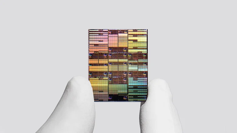
With its new"nanostack" architecture, IBM was able to fit 2 billion transistor into a chip the size of a fingernail.

IBM

IBM claims it has delivered a step change in chip technology after creating the world's first sub-1 nanometer (nm) chip

Building on the "nanosheet" architecture the company used in 2021 create a 2nm chip, IBM says its new "nanostack" design allowed it go even further and make a functioning 7 angstrom (or 0.7nm) chip. The result is a piece of silicon with twice the density of its previous 2nm design, packing nearly 100 billion transistors into a chip the size of a human fingernail. In practical terms, IBM says those additional transistors translate to a chip that offers either a "up to 50 percent more performance, or 70 percent greater energy efficiency than IBM's 2 nm node chips." 

Jay Gambetta, director of IBM Research,  said the new architecture would enable "a future where computing becomes significantly more powerful without a corresponding increase in energy."

The new nanostack architecture sees IBM building on its existing nanosheet transistor technology. The company found it could vertically stack and stagger those transistors. As depicted in the diagram below, each transistor is made up of three nanosheet elements that are approximately five nanometers thick, with about nine nanometers separating each of them. For further context, each nanosheet is made up of only 15 rows of silicon atoms. 
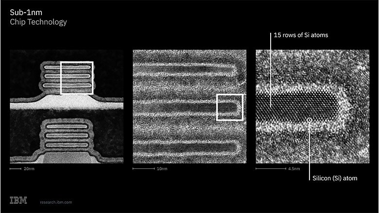
A diagram demonstrating IBM's new nanostack architectureIBM

IBM estimates it will take about five years before nanostack chips enter mass production. At the start of the year, Rapidus — the Japanese chipmaker the company partnered with to commercialize its existing nanosheet technology — said it was aiming to start producing 2nm chips at scale by the second half 2027, making the five-year estimate feel overly optimistic. 

IBM said it would share more information about its commercialization plans in the future, but the company was adamant its new architecture would create a path for chipmakers to continue making more powerful and efficient silicon for at least the next decade.