





Posted on søndag, april 20, 2025 in Hal9k, Planets
As I’ve written about previously I have had the Olimex A20-OLinuXino-LIME2 in service for quite some time. But one thing that I’ve been curious about is why it’s only available with 1GB of RAM, when the A20 chip itself can support up to 2GB? Could it be upgraded to 2GB RAM by a simple swap in of a larger memory module?
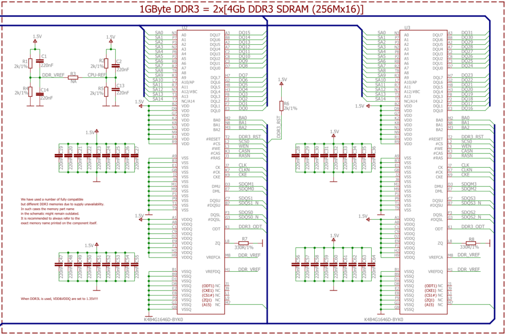
If you check the schematic the address lines are actually wired up: both A14 and A15 which are labelled NC (no-connect) on the chips are wired up on the address bus, meaning a full 2¹⁶ row addresses should be addressable. So this might actually work out!
From a very high level the way a CPU accesses memory is the same all the way from a small microprocessor like the RP2040 up to a x86. There are a number of pins connecting the CPU and the RAM:
The most crude form of using more than one RAM chip would be to use “chip select” as known from SPI or I2C communication. This is however not how it’s done on the LIME2: address, data and chip select lines are wired in parallel for the two chips. The only difference in wiring is on the “DMU”, “DML”, and “DQSU” and “DQSL” lines: these are used for lower and upper byte data strobes, meaning that the same address is setup for both chips, and then the chips are strobed one at a time – effectively allowing each chip to prepare the read in parallel.
Luckily DDR chips are standardized, but it seems that the standardisation does not quite go all the way to the datasheets, in e.g. pin naming and concepts. But at least the density and organization are standardised: the 256M is the number of different addressable storage locations, and the x16 is how many bits are stored per location. Multiplying those gives the number of megabits stored, 4096 megabits in this case, so dividing by 8 gives the number of megabytes stored: 512MiB.
Looking at the pinout for the specified chip (K4B4G1646D-BYK0, a Samsung chip):
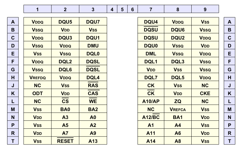
We can see it specifies only address lines A0–A14, which is enough for a 256M module. But the LIME2 schematic was helpful enough to hookup A15 to the JEDEC standard location, even if that pin is NC on all memory modules shipped. This might actually work!
The last crucial parameter for selecting bigger RAM chips is the supply voltage. DDR3 comes in both standard and low-voltage (DDR3L) variants. The LIME2 schematic actually just specifies that “When DDR3L is used, VDD&VDDQ are set to 1.35V!!!“, so to know which it is we would have to look at the particular board and measure the power supply line. But luckily, almost all DDR3L chips are backwards compatible to the 1.5V DDR3 level, so as long as we can find a DDR3L chip voltage shouldn’t be an issue.
So in theory any 512Mx16 DDR3L chip should work. In practice I ended up trying two variants:
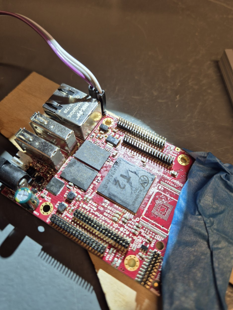
Finally, we can jump to the microscope soldering station, and learn to BGA solder. This was by far the longest part of this project. The chips come pre-balled, so in theory the job could have been as simple as desoldering the old chips and soldering on the new ones. Not so easy in practice. I ended up having to re-ball and re-solder chips, apply flux, solder-wick and ethanol in copious amount, re-attach SMD resistors that had taken a stroll under the heatgun, and battling a self-compiled U-Boot that I probably messed up badly. You get to see my frustration in a few nice pictures.
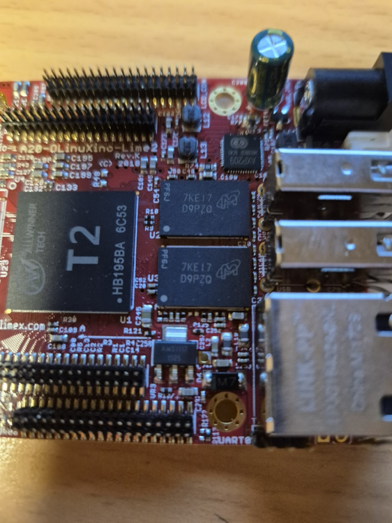
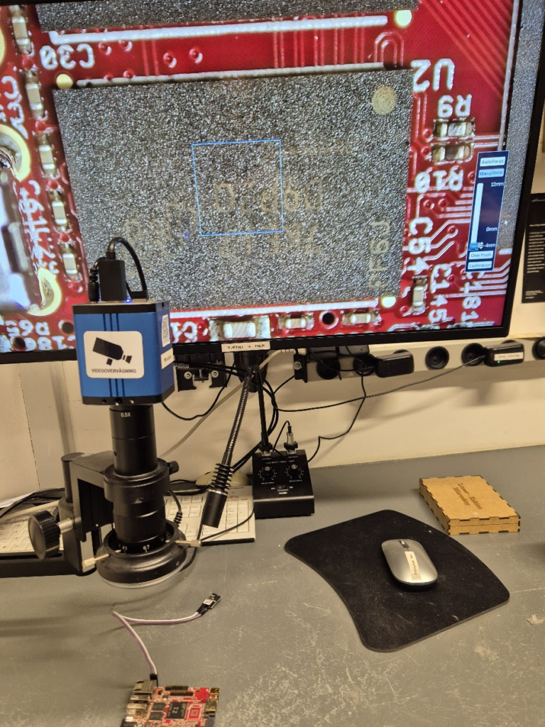
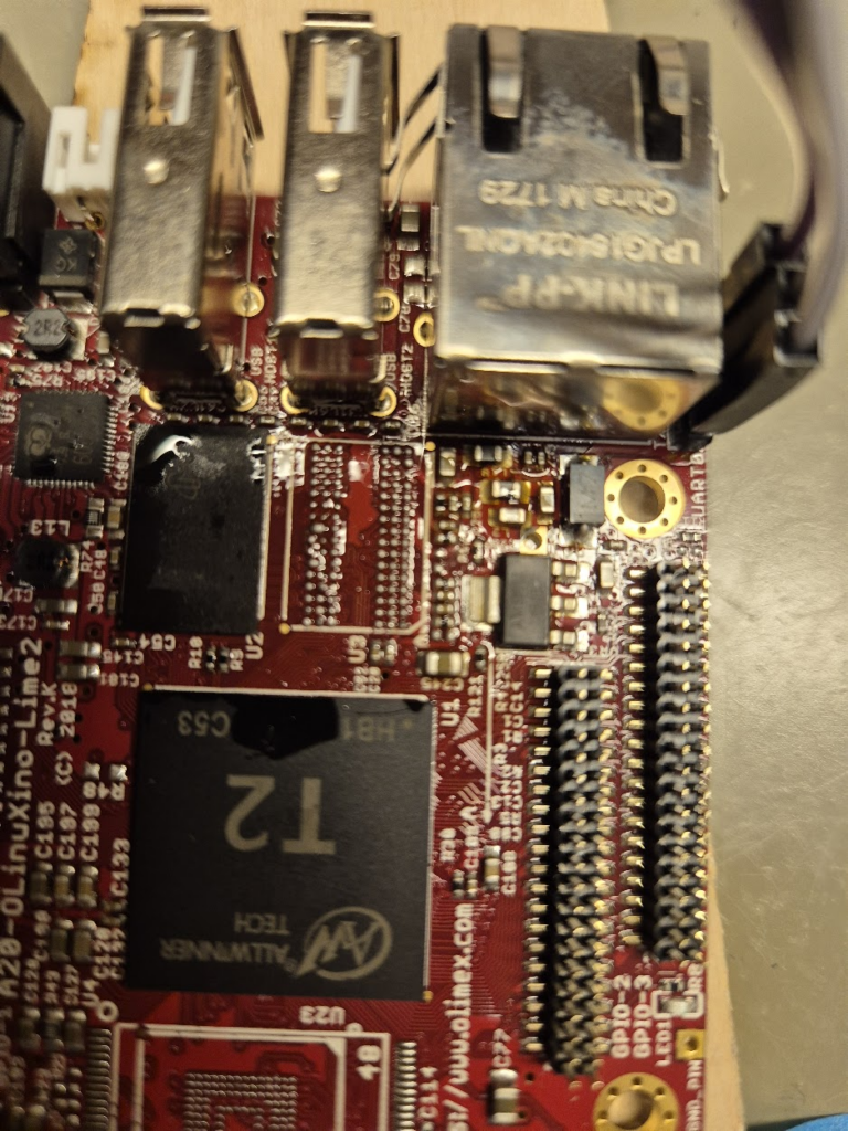
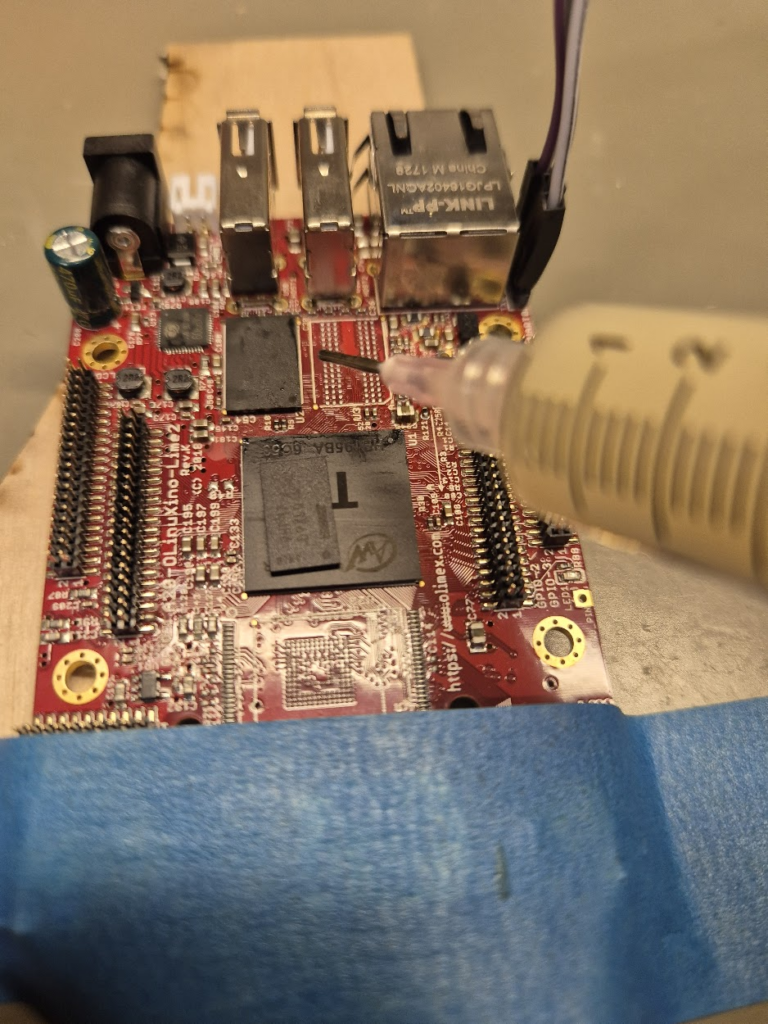
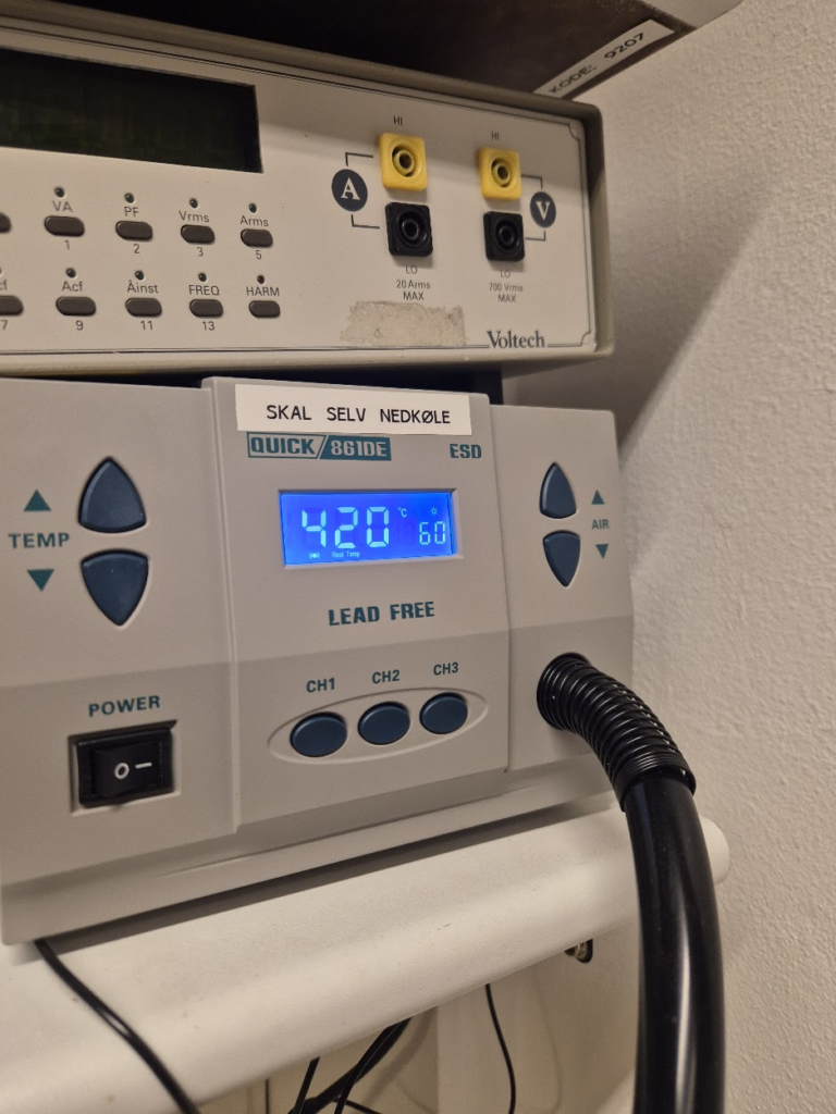
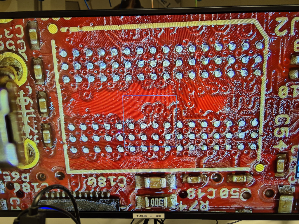
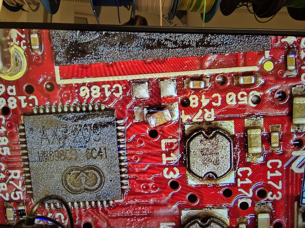
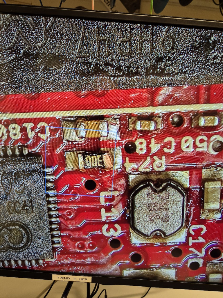
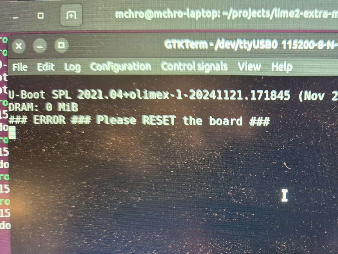
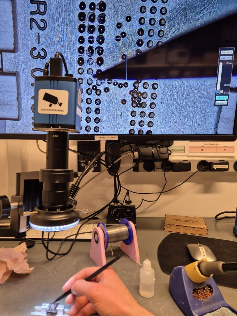
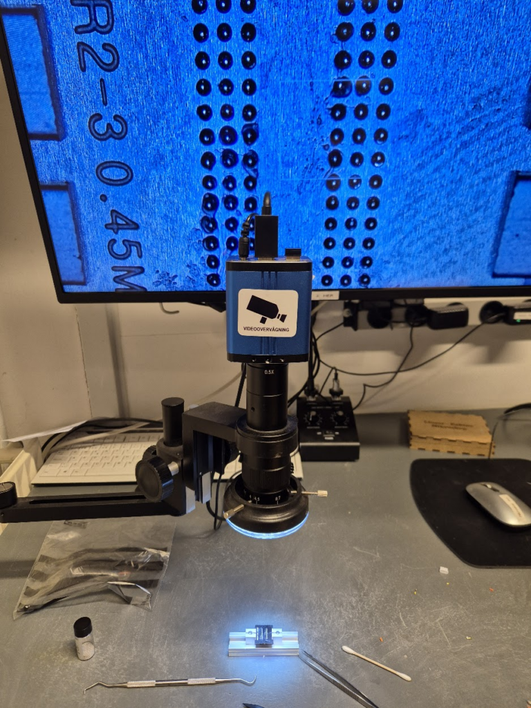
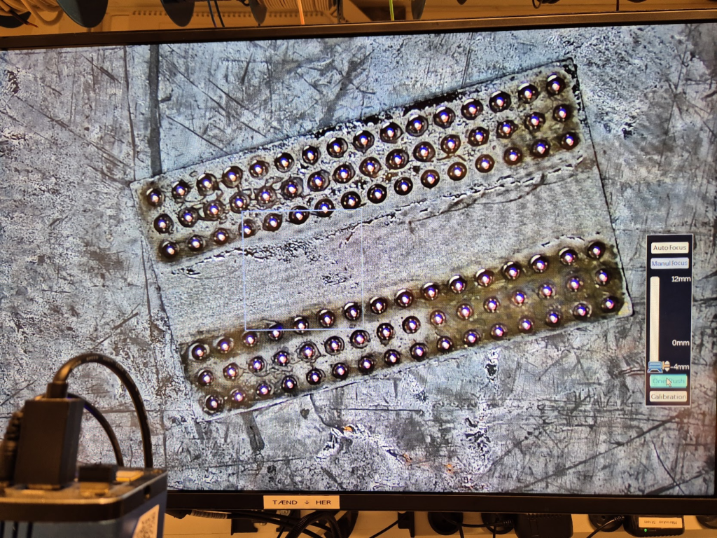
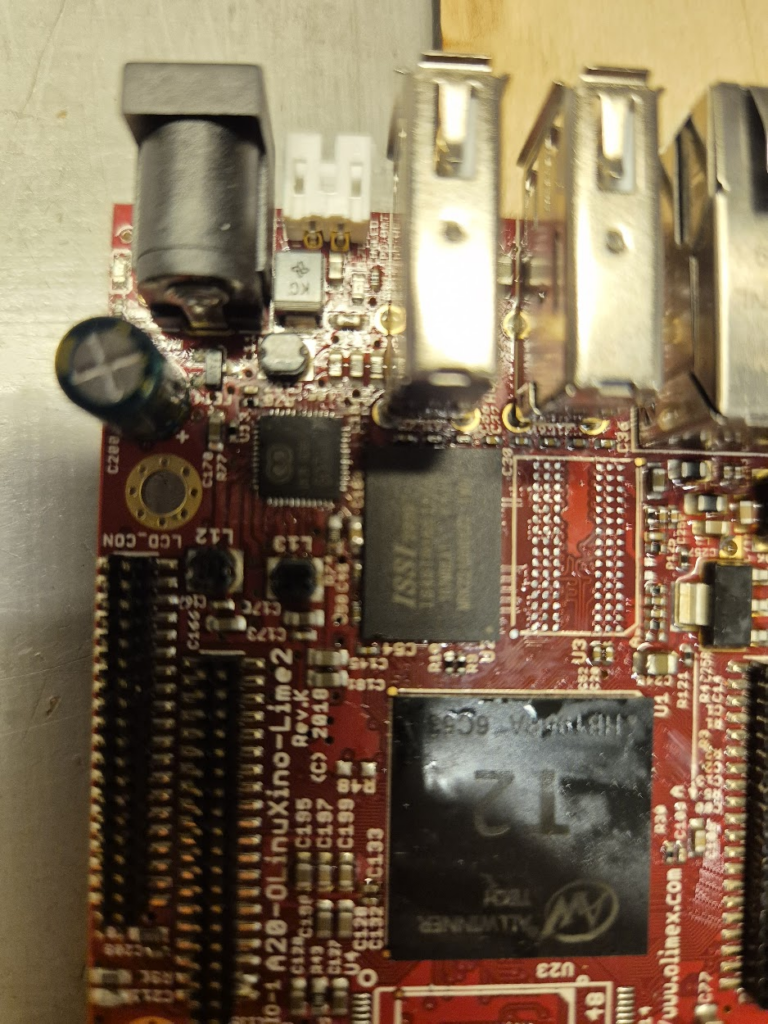
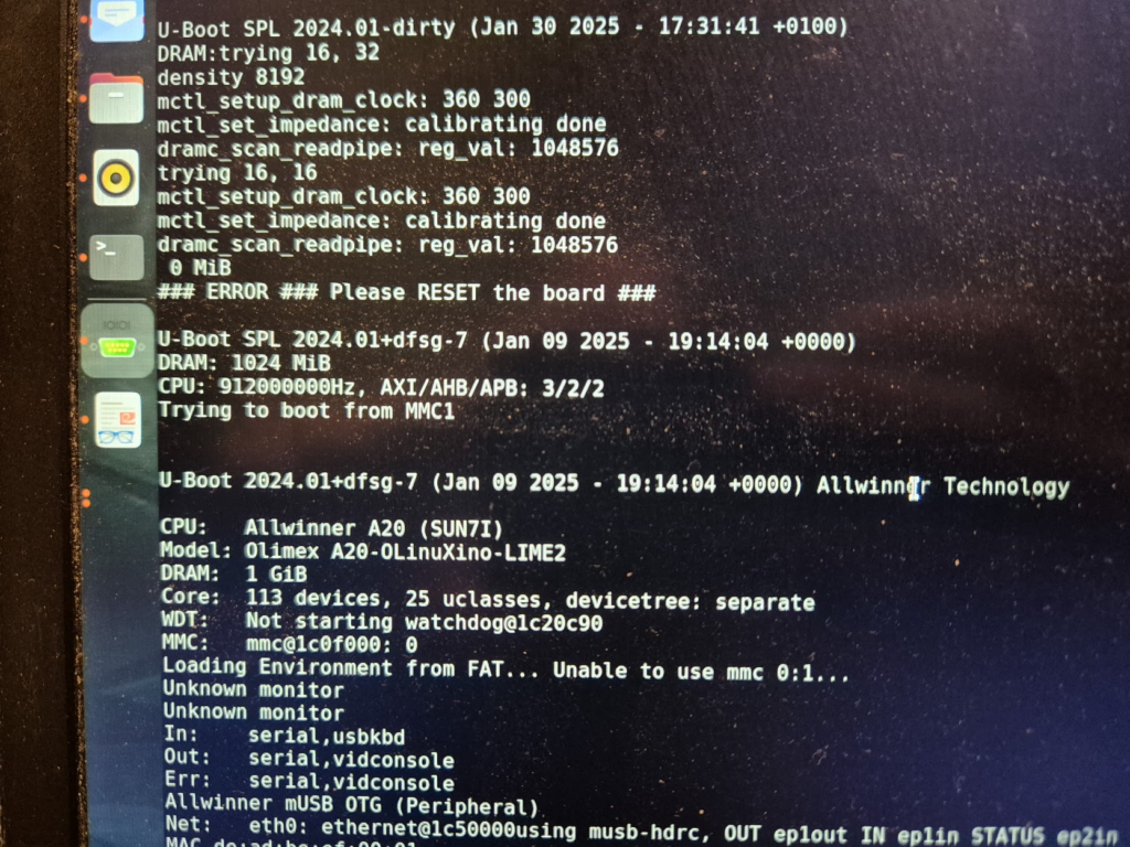
I have a suspicion that I messed up U-Boot at one point, by trying to compile it with automatic impedance calibration, instead of leaving the LIME2 defaults DDR settings in. This might be the reason I couldn’t get the Micron MT41K512M16 chips to work, but I will have to investigate this more. I probably also messed up the first soldering on of a chip, by not using enough heat. My main piece of advice would be to not be too afraid to get the temperature of the chip up, if you spend more than about a minute trying to solder or desolder the chip, chances are you will be heating up the rest of the board much more than needed and the chip itself too little!
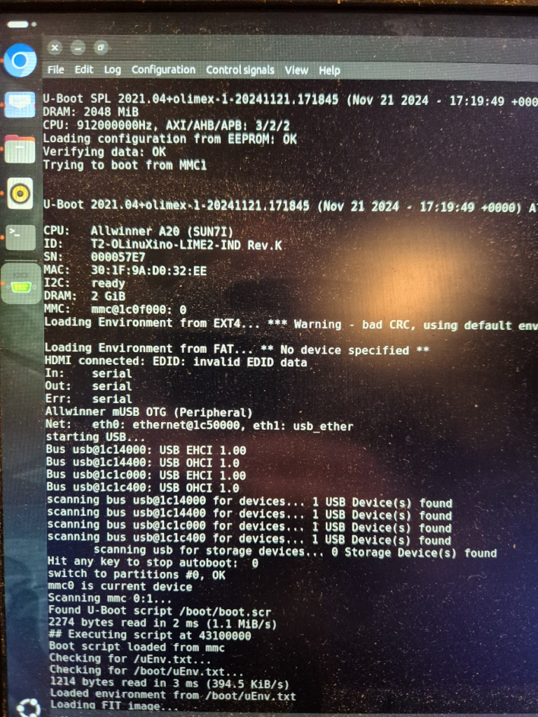
The moment of seeing the board booting with 1GB from a single ISSI IS46TR16512BL was a great success though — soldering on the other ISSI chip was basically a walk in the park.
A serial terminal is absolutely essential for getting any kind of feedback on the early part of the boot process, and the first user-controlled software encountered on the LIME2 is U-Boot. U-Boot is the universal bootloader responsible for figuring out the basic hardware configuration (including RAM configuration), finding the (Linux) kernel and moving it into RAM and giving over control to the kernel for further booting. Curiously, U-Boot can run with absolutely no RAM chips (guess how I know!), because the SunXi early boot process happens entirely in on-chip ROM and a small on-chip SRAM.
But how does U-Boot actually determine how much memory is there? Well, remember that accessing a memory location is just putting an address on the address lines and pulling some signalling pins. So U-Boot simply tries and write to increasing addresses and see if the expected data can be read back. How is the memory size then communicated to the Linux kernel? By a bootarg parameter, e.g. mem=2048M. Does this mean we can try and trick the Linux kernel into thinking it has more memory than physically present? Yes, but with disastrous results if the non-existent memory is ever attempted to be used.
Until told otherwise, I will happily claim that this is the only 2GB LIME2 in existence — but do let me know if you give the procedure a try! In the end the process was much simpler than I thought: the tricky part was definitely getting the hang of BGA soldering. Don’t be afraid of raising the temperature! Peeking into the innards of U-Boot was also fascinating: there is definitely a layer below of pretty dark bit-setting magic, but the overall process is really well structured!
此内容由惯性聚合(RSS阅读器)自动聚合整理,仅供阅读参考。 原文来自 — 版权归原作者所有。