





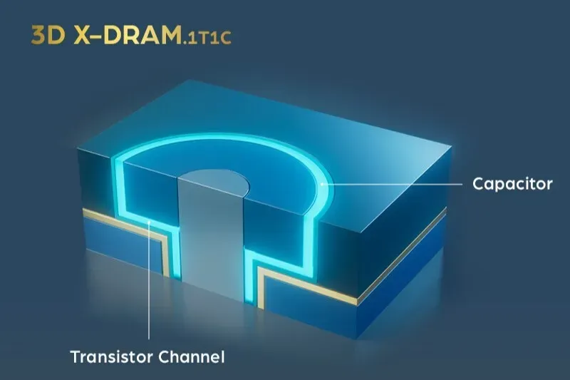
NEO Semiconductor announced on April 23rd that its 3D X-DRAM technology has successfully passed proof-of-concept (POC) validation, demonstrating that a new class of high-density DRAM can be manufactured using existing 3D NAND infrastructure. The company simultaneously announced a new strategic investment led by Stan Shih, founder and former Chairman and CEO of Acer, and a board director of TSMC for over two decades.
At the center of the announcement is the company’s 3D X-DRAM technology, a new class of DRAM that aims to break past conventional memory scaling limits by adopting a vertically stacked architecture designed for higher density, lower power consumption, and improved suitability for AI-driven workloads.
Article continues below
The proof-of-concept chips, fabricated and tested at Taiwan's National Institutes of Applied Research - Taiwan Semiconductor Research Institute (NIAR-TSRI) in collaboration with National Yang Ming Chiao Tung University, delivered the following results:
Read/write latency: under 10 nanoseconds
Data retention: over 1 second at 85°C/185°F (claimed 15× improvement over JEDEC standard)
Bit-line disturbance: over 1 second at 85°C (185°F)
Word-line disturbance: over 1 second at 85°C
Endurance: greater than 10¹⁴ cycles
Industry commentary included in the announcement was quite positive — although this does not imply confirmation of viability at scale. TechInsights’ Jeongdong Choe described the results as a “significant milestone” in the shift toward 3D memory architectures, noting that conventional DRAM scaling is approaching physical limits and that the industry is increasingly exploring vertical alternatives.
The broader context behind this development is the growing strain AI workloads are placing on memory systems. While GPU compute performance has scaled aggressively over the past decade, memory bandwidth — the rate at which data can be fed to those processors — has become a limiting factor in large-scale AI training and inference systems. This has already driven widespread adoption of high-bandwidth memory (HBM), a vertically stacked DRAM architecture integrated close to GPUs. However, HBM presents complex 3D stacking and bonding requirements and high manufacturing costs.
Quick clarification sidebar: 3D X-DRAM and HBM both use vertical stacking concepts, but they stack different things in different ways. HBM stacks multiple finished DRAM dies on top of each other, then connects them with through-silicon vias (TSVs) and places them beside/near a GPU or CPU on an interposer. 3D X-DRAM, based on NEO’s claims. aims to build memory cells in a 3D NAND-like monolithic vertical structure, where layers are fabricated as part of the memory array itself rather than stacking separate packaged DRAM dies.
3D X-DRAM is just one of several technologies under development to address the AI memory problem. Just a day before NEO Semiconductor’s announcement, we reported that SAIMEMORY and its ZAM architecture, backed by SoftBank and Intel with Japanese government support, is pursuing a similar goal on a parallel track.
NEO Semiconductor’s device successfully passed extensive electrical and reliability evaluations, confirming the robustness and stability of the proposed memory architecture. It is important to reiterate that this is a proof of concept, not a production-ready memory chip. The road from validated POC to commercial volume is long — and littered with the remains of promising memory technologies that never made it out of the lab. However, with NEO Semiconductor's usage of established 3D NAND processes, the future is bright.
"The successful proof-of-concept not only demonstrates the potential of innovative memory architectures, but also confirms the feasibility of implementing advanced memory technologies using mature processes. This collaboration among NEO, NYCU IAIS, and NIAR-TSRI further underscores the value of industry–academia partnerships in accelerating innovation from concept to practical implementation," said Jack Sun, Senior Vice President of NYCU and Dean of IAIS, and former CTO of TSMC

Follow Tom's Hardware on Google News, or add us as a preferred source, to get our latest news, analysis, & reviews in your feeds.